
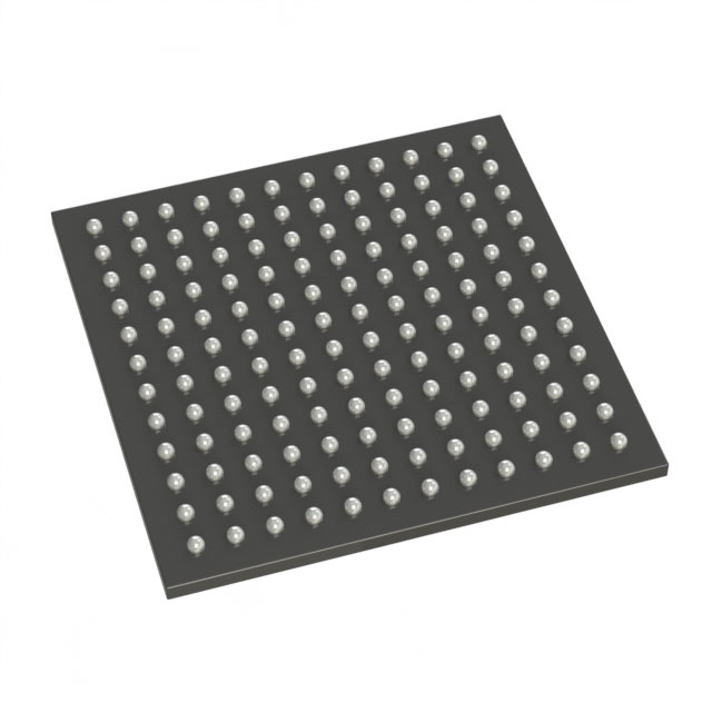
A54SX08-1FG144I
| Part Description |
SX Field Programmable Gate Array (FPGA) IC 111 144-LBGA |
|---|---|
| Quantity | 286 Available (as of June 15, 2026) |

| Product Category | Field Programmable Gate Array (FPGA) |
|---|---|
| Manufacturer | Microchip Technology |
| Manufacturing Status | Active |
| Manufacturer Standard Lead Time | 52 Weeks |
| Datasheet |
Specifications & Environmental
| Device Package | 144-FPBGA (13x13) | Grade | Industrial | Operating Temperature | -40°C – 85°C | ||
|---|---|---|---|---|---|---|---|
| Package / Case | 144-LBGA | Number of I/O | 111 | Voltage | 3 V - 5.5 V | ||
| Mounting Method | Surface Mount | RoHS Compliance | RoHS non-compliant | REACH Compliance | REACH Unaffected | ||
| Moisture Sensitivity Level | 3 (168 Hours) | Number of LABs/CLBs | 768 | Number of Logic Elements/Cells | 768 | ||
| Number of Gates | 12000 | ECCN | 3A991D | HTS Code | 8542.39.0001 | ||
| Qualification | N/A |
Overview of A54SX08-1FG144I – SX Field Programmable Gate Array (FPGA) IC 111 144-LBGA
The A54SX08-1FG144I is a nonvolatile SX family FPGA offering a compact, surface-mount 144-LBGA package with industrial-grade operation. It delivers 12,000 system gates implemented across 768 logic elements and provides 111 user I/Os for mixed-voltage interfacing.
Designed for embedded systems and industrial electronics, this device combines deterministic timing, flexible I/O support and on-chip security features to simplify board-level design and in-system configuration.
Key Features
- Core Capacity — 12,000 system gates implemented as approximately 768 logic elements, suitable for moderate-density glue logic, protocol bridges and control functions.
- High-Speed Performance — SX family documented system performance up to 250 MHz and internal performance up to 350 MHz for timing-critical paths.
- I/O Flexibility — 111 user I/Os with configurable support for multiple standards including 3.3 V/5 V PCI, 5 V TTL, 3.3 V LVTTL and 2.5 V LVCMOS2; supports mixed-voltage operation with 5 V input tolerance and 5 V drive strength.
- Nonvolatile Single-Chip Solution — On-chip nonvolatile configuration removes the need for an external configuration PROM, simplifying BOM and power-up behavior.
- Robust System Features — Hot-swap compliant I/Os, configurable weak pull-up/pull-down at power-up, individual output slew-rate control, and deterministic, user-controllable timing.
- Security & Test — Actel Secure Programming Technology with FuseLock prevents reverse engineering; boundary-scan testing compliant with IEEE 1149.1 (JTAG) and in-system diagnostic/verification via Silicon Explorer II.
- Package & Mounting — Surface-mount 144-LBGA (supplier package: 144-FPBGA (13x13)), enabling compact board designs.
- Voltage & Temperature — Wide supply range from 3 V to 5.5 V and industrial operating temperature range of −40 °C to 85 °C.
Typical Applications
- Industrial Control — Implement deterministic control logic and protocol conversion for factory automation and motor control systems that require industrial temperature operation.
- Interface Bridging — Use the flexible I/O and mixed-voltage support to build PCI or legacy interface bridges and board-level translators.
- Embedded Instrumentation — Integrate custom signal processing, control sequencing, and I/O aggregation in test and measurement equipment.
- Secure Systems — Leverage on-chip nonvolatile configuration and FuseLock technology for designs that require protection against reverse engineering and secure in-field updates.
Unique Advantages
- Single-Chip Nonvolatile Configuration: Eliminates external configuration memory and simplifies power-up sequencing and board-level BOM.
- Flexible, Mixed-Voltage I/O: Reduces the need for level translators by supporting multiple I/O standards and 5 V tolerance/drive.
- Deterministic Timing Control: User-controllable timing features help designers meet tight timing budgets without guesswork.
- Security Built In: FuseLock secure programming technology provides protection against reverse engineering and unauthorized readback.
- Industrial Ready: Rated for operation from −40 °C to 85 °C and a wide 3 V to 5.5 V supply range for reliable operation in industrial environments.
Why Choose A54SX08-1FG144I?
The A54SX08-1FG144I positions itself as a practical, nonvolatile FPGA option for designers needing moderate logic density (12,000 system gates / 768 logic elements) and extensive I/O flexibility in a compact 144-LBGA footprint. Its combination of mixed-voltage I/O support, on-chip security, deterministic timing and industrial temperature rating makes it well suited to embedded control, interface bridging and secure instrumentation applications.
Backed by the SX family feature set — including in-system diagnostic capabilities and IEEE 1149.1 boundary-scan — this device offers a balanced mix of performance, integration and system-level features to reduce board complexity and accelerate development.
Request a quote or submit an inquiry to receive pricing and availability for the A54SX08-1FG144I. Our team will respond with ordering and support information tailored to your project requirements.


Date Founded: 1989
Headquarters: Chandler, Arizona, USA
Employees: 22,000+
Revenue: $8.349 Billion
Certifications and Memberships: ISO9001:2015, IATF16949:2016, AS 9100D


