
A54SX08-1FGG144I
| Part Description |
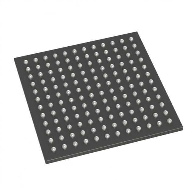
SX Field Programmable Gate Array (FPGA) IC 111 144-LBGA |
|---|---|
| Quantity | 1,435 Available (as of June 18, 2026) |

| Product Category | Field Programmable Gate Array (FPGA) |
|---|---|
| Manufacturer | Microchip Technology |
| Manufacturing Status | Active |
| Manufacturer Standard Lead Time | 52 Weeks |
| Datasheet |
Specifications & Environmental
| Device Package | 144-FPBGA (13x13) | Grade | Industrial | Operating Temperature | -40°C – 85°C | ||
|---|---|---|---|---|---|---|---|
| Package / Case | 144-LBGA | Number of I/O | 111 | Voltage | 3 V - 5.5 V | ||
| Mounting Method | Surface Mount | RoHS Compliance | ROHS3 Compliant | REACH Compliance | REACH Unaffected | ||
| Moisture Sensitivity Level | 3 (168 Hours) | Number of LABs/CLBs | 768 | Number of Logic Elements/Cells | 768 | ||
| Number of Gates | 12000 | ECCN | 3A991D | HTS Code | 8542.39.0001 | ||
| Qualification | N/A |
Overview of A54SX08-1FGG144I – SX Field Programmable Gate Array (FPGA) IC 111 144-LBGA
The A54SX08-1FGG144I is a nonvolatile SX family FPGA supplied by Microchip Technology, delivered in a compact 144-ball LBGA package for surface-mount assembly. It provides a field-programmable logic platform with 12,000 system gates and 768 logic elements, plus 111 user I/Os, targeted at industrial and embedded control applications.
Built on the SX-A family architecture, the device offers high internal performance and predictable timing characteristics while supporting mixed-voltage I/O and power-up/down friendly operation, making it suitable for designs that require low board-level configuration overhead and I/O flexibility.
Key Features
- Logic Capacity — 12,000 system gates and 768 logic elements for implementing control, glue logic, finite state machines, and small-scale datapaths.
- I/O Count & Flexibility — 111 user I/Os with configurable support for multiple interface voltages; ideal for multi-voltage systems and interface bridging.
- Voltage Supply — Operates from 3 V to 5.5 V, enabling compatibility with a broad range of system power rails.
- No On-Chip RAM — 0 total RAM bits (no embedded RAM), suitable for logic-centric designs that rely on external memory or do not require embedded block RAM.
- Performance — SX-A family performance characteristics include up to 250 MHz system performance and up to 350 MHz internal performance for timing-critical paths.
- I/O and Interface Support — Hot-swap compliant I/Os, configurable I/O for 3.3 V / 5 V PCI, 5 V TTL, 3.3 V LVTTL, and 2.5 V LVCMOS2; supports mixed 2.5 V, 3.3 V, and 5 V operation with 5 V input tolerance and 5 V drive strength.
- Nonvolatile, Single-Chip Solution — Single-chip configuration (nonvolatile) removes the need for external configuration memory and simplifies system initialization.
- Package & Mounting — 144-LBGA package (supplier package: 144-FPBGA 13×13), surface-mount mounting for compact PCB implementations.
- Industrial Temperature Grade — Rated for operation from −40 °C to +85 °C.
- Standards, Test & Security — 66 MHz PCI compliance, boundary-scan testing (IEEE 1149.1 JTAG), deterministic timing, in‑system diagnostics, and secure programming capability with FuseLock technology.
- Regulatory — RoHS compliant.
Typical Applications
- Industrial Control — Implement control logic, signal conditioning, and interface glue in industrial systems where extended temperature range and mixed-voltage I/O are required.
- Interface Bridging — Translate or aggregate signals between different voltage domains and legacy/modern interfaces using the device's configurable I/Os and 111 available pins.
- Embedded System Glue Logic — Replace discrete logic, microcontroller peripherals, or CPLDs with a single nonvolatile FPGA to reduce board complexity and BOM count.
- Secure Logic and Functionality — Use the device’s secure programming technology and boundary-scan support to protect and validate in-system logic implementations.
Unique Advantages
- Compact, Surface-Mount Footprint: 144-LBGA package enables higher-density PCB layouts while preserving 111 user I/Os.
- Nonvolatile Single-Chip Design: Eliminates external configuration memory, simplifying power-up behavior and reducing board-level components.
- Flexible I/O Voltage Support: Configurable interface levels (2.5 V, 3.3 V, 5 V) and 5 V tolerant inputs provide compatibility across mixed-voltage systems.
- Industrial Temperature Rating: −40 °C to +85 °C operation supports deployment in industrial and outdoor environments.
- Predictable, High-Speed Operation: SX-A family timing and performance characteristics (250 MHz system, 350 MHz internal) support timing-critical designs.
- Built-in Test and Security Features: Boundary-scan JTAG, in-system diagnostics, and secure programming (FuseLock) streamline manufacturing test and protect IP.
Why Choose A54SX08-1FGG144I?
The A54SX08-1FGG144I delivers a compact, nonvolatile FPGA solution with 12,000 system gates, 768 logic elements and 111 user I/Os in a 144-LBGA package. Its mixed-voltage I/O capability, broad supply range (3 V to 5.5 V), and industrial temperature rating make it a practical choice for embedded and industrial designs that require flexible interfacing and reliable operation across environments.
As part of the SX-A family, the device benefits from deterministic timing, built-in testability and secure programming features, offering designers a straightforward way to implement control logic, interface bridging and secure in-system functions without external configuration components.
Request a quote or submit an inquiry to receive pricing and availability for the A54SX08-1FGG144I.


Date Founded: 1989
Headquarters: Chandler, Arizona, USA
Employees: 22,000+
Revenue: $8.349 Billion
Certifications and Memberships: ISO9001:2015, IATF16949:2016, AS 9100D


