
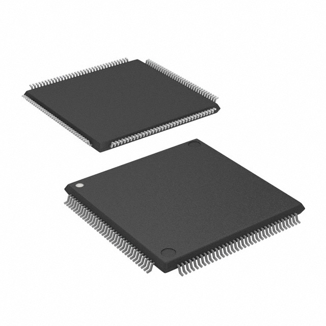
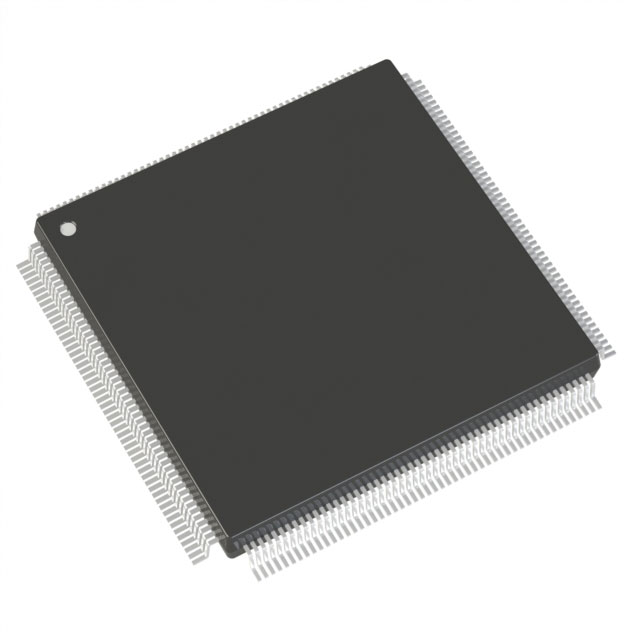
A54SX32-2BGG329I
| Part Description |
SX Field Programmable Gate Array (FPGA) IC 249 329-BBGA |
|---|---|
| Quantity | 651 Available (as of June 14, 2026) |

| Product Category | Field Programmable Gate Array (FPGA) |
|---|---|
| Manufacturer | Microchip Technology |
| Manufacturing Status | Active |
| Manufacturer Standard Lead Time | 20 Weeks |
| Datasheet |
Specifications & Environmental
| Device Package | 329-PBGA (31x31) | Grade | Industrial | Operating Temperature | -40°C – 85°C | ||
|---|---|---|---|---|---|---|---|
| Package / Case | 329-BBGA | Number of I/O | 249 | Voltage | 3 V - 5.5 V | ||
| Mounting Method | Surface Mount | RoHS Compliance | ROHS3 Compliant | REACH Compliance | REACH Unaffected | ||
| Moisture Sensitivity Level | 3 (168 Hours) | Number of LABs/CLBs | 2880 | Number of Logic Elements/Cells | 2880 | ||
| Number of Gates | 48000 | ECCN | 3A991D | HTS Code | 8542.39.0001 | ||
| Qualification | N/A |
Overview of A54SX32-2BGG329I – SX Field Programmable Gate Array (FPGA) IC 249 329-BBGA
The A54SX32-2BGG329I is a nonvolatile SX-A family FPGA from Microchip Technology, delivered in a 329-ball BGA package with surface-mount construction and industrial temperature rating (‑40 °C to 85 °C). It provides a mid-range logic capacity and high I/O density for system designs that require configurable logic, deterministic timing and mixed-voltage I/O support.
Built for applications that demand a combination of integration and reliable operation, this device combines approximately 48,000 system gates with 2,880 logic elements and 249 user-programmable I/O pins in a RoHS-compliant package.
Key Features
- Core performance: System performance up to 250 MHz and internal performance up to 350 MHz as specified for the SX-A family, supporting responsive logic operation.
- Logic capacity: Approximately 48,000 system gates and 2,880 logic elements, providing mid-range programmable logic density for control, glue-logic and interface functions.
- I/O density and flexibility: 249 user I/O pins with configurable I/O support for multiple voltage standards and mixed-voltage operation (2.5 V, 3.3 V, 5 V); device-level supply support from 3 V to 5.5 V.
- Nonvolatile single-chip configuration: Single-chip, nonvolatile architecture eliminates the need for external configuration memory and enables immediate functional availability after power-up.
- Power and system friendliness: Hot-swap compliant I/Os and power-up/power-down friendly operation with no sequencing required for supply voltages, simplifying system power management.
- System interfaces and standards: SX-A family support for 66 MHz PCI and IEEE 1149.1 boundary-scan (JTAG) testing provides protocol and testability options for system integration.
- Security and diagnostics: Secure programming technology with FuseLock™ protection and in-system diagnostic/verification capability (Silicon Explorer II) as provided in SX-A family documentation.
- Package and environmental: 329-ball BBGA package (supplier package: 329-PBGA, 31×31), surface mount, RoHS compliant, and industrial temperature grade (‑40 °C to 85 °C).
Typical Applications
- Industrial control and automation: High I/O count and industrial temperature rating support sensor interfacing, I/O aggregation and real-time control logic in factory and process equipment.
- Mixed-voltage interface bridging: Configurable I/O with 2.5 V/3.3 V/5 V support enables board-level protocol conversion and signal translation without extensive level-shifter circuitry.
- PCI-based systems and legacy interfaces: Family-level support for 66 MHz PCI makes the device suitable for designs that require legacy PCI connectivity and related glue logic.
- Embedded systems with immediate availability: Nonvolatile single-chip configuration eliminates external configuration storage, simplifying boot behavior in embedded products.
Unique Advantages
- Nonvolatile integration: On-chip nonvolatile configuration removes the need for external configuration PROMs, reducing BOM and board complexity.
- High I/O per package: 249 user I/Os in a 329-ball BGA provides dense I/O routing capability for complex interfacing without increasing package count.
- Mixed-voltage I/O support: Native support for 2.5 V, 3.3 V and 5 V interfaces reduces the need for external level-shifting and simplifies multi-voltage board designs.
- Industrial temperature grade: Qualified for operation from ‑40 °C to 85 °C, enabling deployment in industrial environments and equipment.
- Built-in test and security: JTAG boundary-scan and FuseLock secure programming provide testability and design protection options for production and field service.
- Power-up friendly I/Os: Hot-swap compliance and no required supply sequencing reduce power-management constraints during system integration.
Why Choose A54SX32-2BGG329I?
The A54SX32-2BGG329I delivers a balanced combination of mid-range logic capacity, high I/O density and nonvolatile configuration in a single, industrial-grade BGA package. Its mixed-voltage I/O capabilities, hot-swap friendliness and family-level support for PCI and JTAG make it suitable for embedded and industrial designs that require robust interfacing, deterministic timing and simplified system-level power sequencing.
This device is a practical choice for design teams looking to reduce external components, simplify board-level voltage management and maintain secure, testable programmable logic in industrial-temperature applications, while taking advantage of established SX-A family features and tooling.
Request a quote or submit an RFQ to evaluate the A54SX32-2BGG329I for your next design.


Date Founded: 1989
Headquarters: Chandler, Arizona, USA
Employees: 22,000+
Revenue: $8.349 Billion
Certifications and Memberships: ISO9001:2015, IATF16949:2016, AS 9100D


