
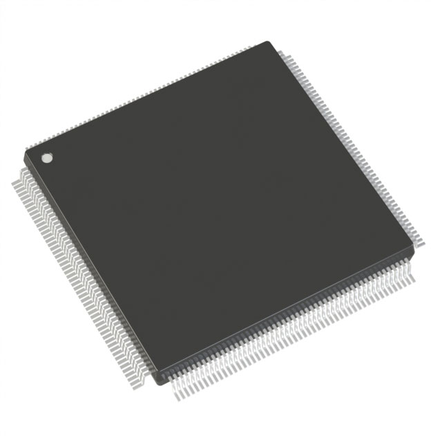
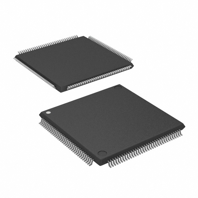
A54SX32-2PQ208
| Part Description |
SX Field Programmable Gate Array (FPGA) IC 174 208-BFQFP |
|---|---|
| Quantity | 371 Available (as of June 18, 2026) |
| Product Category | Field Programmable Gate Array (FPGA) |
|---|---|
| Manufacturer | Microchip Technology |
| Manufacturing Status | Obsolete |
| Manufacturer Standard Lead Time | Contact Us |
| Datasheet |
Specifications & Environmental
| Device Package | 208-PQFP (28x28) | Grade | Commercial | Operating Temperature | 0°C – 70°C | ||
|---|---|---|---|---|---|---|---|
| Package / Case | 208-BFQFP | Number of I/O | 174 | Voltage | 3 V - 5.25 V | ||
| Mounting Method | Surface Mount | RoHS Compliance | RoHS non-compliant | REACH Compliance | REACH Unaffected | ||
| Moisture Sensitivity Level | 3 (168 Hours) | Number of LABs/CLBs | 2880 | Number of Logic Elements/Cells | 2880 | ||
| Number of Gates | 48000 | ECCN | 3A991D | HTS Code | 8542.39.0001 | ||
| Qualification | N/A |
Overview of A54SX32-2PQ208 – SX Field Programmable Gate Array (FPGA) IC 174 208-BFQFP
The A54SX32-2PQ208 is a commercial-grade, nonvolatile SX family FPGA from Microchip Technology designed for mixed-voltage, high-integration applications. It provides 48,000 system gates and 2,880 logic elements in a 208-pin surface-mount package with 174 user I/Os, making it suitable for compact commercial embedded designs that require flexible I/O and deterministic timing.
Built on the SX-A family architecture, this device supports up to 250 MHz system performance and up to 350 MHz internal performance, configurable I/O standards, and secure programming features—delivering a compact, single-chip programmable logic solution for a variety of commercial applications.
Key Features
- Capacity and Logic — 48,000 system gates and approximately 2,880 logic elements provide substantive logic density for glue logic, control, and mid-complexity designs.
- I/O and Voltage Flexibility — 174 user I/Os with configurable support for 3.3 V / 5 V PCI, 5 V TTL, 3.3 V LVTTL, and 2.5 V LVCMOS2; supports mixed-voltage operation and 5 V input tolerance.
- Performance — Family-level specifications include up to 250 MHz system performance and up to 350 MHz internal performance for time-critical logic paths.
- Nonvolatile Single-Chip Configuration — On-chip nonvolatile configuration removes the need for external bitstream memory and simplifies system startup; power-up/down friendly with no supply sequencing required.
- Security and Test — Actel Secure Programming Technology (FuseLock™) for protection against reverse engineering, plus IEEE 1149.1 JTAG boundary-scan for board-level testing and diagnostics.
- In-System Diagnostics — Supports in-system diagnostic and verification capabilities (Silicon Explorer II) to streamline bring-up and debugging.
- Package and Mounting — 208-pin BFQFP package (supplier device package: 208-PQFP, 28 × 28) in a surface-mount form factor for compact PCB designs.
- Power and Temperature — Wide supply range of 3 V to 5.25 V and commercial operating temperature range of 0 °C to 70 °C.
- Regulatory — RoHS compliant.
- Speed Grade — The –2 speed grade indicates approximately 25% faster performance than the standard speed grade for the SX-A family.
- Embedded Memory — No on-chip RAM bits; suitable for applications that utilize external memory or are optimized for minimal embedded RAM usage.
Typical Applications
- Commercial Embedded Systems — Implement control logic, protocol handling, and interface glue in compact commercial products that require configurable I/O and moderate logic density.
- PCI and Bus Interfaces — Use the device’s configurable I/O and PCI-compatible signaling for 3.3 V / 5 V PCI interfacing and bus bridging tasks.
- Security-Conscious Designs — Apply FuseLock™ programming to protect IP in products where design confidentiality is required.
- Test & Measurement Equipment — Leverage deterministic timing and JTAG boundary-scan for reliable instrument control and board-level testability.
Unique Advantages
- Deterministic, User-Controllable Timing: SX family timing architecture provides predictable timing behavior for designs requiring repeatable performance characteristics.
- Single-Chip Nonvolatile Configuration: Eliminates external configuration memory and simplifies system BOM and startup sequencing.
- Flexible Mixed-Voltage I/O: Configurable I/O standards and 5 V tolerance reduce or remove the need for external level translators in mixed-voltage systems.
- Design Protection: FuseLock™ secure programming helps prevent reverse engineering and protects IP in the field.
- Built-In Test and Debug Support: JTAG boundary-scan plus Silicon Explorer II diagnostics streamline bring-up, in-system verification, and fault isolation.
- RoHS Compliant Commercial Option: Meets RoHS requirements and is targeted for commercial-temperature applications (0 °C to 70 °C).
Why Choose A54SX32-2PQ208?
The A54SX32-2PQ208 positions itself as a compact, secure, and flexible FPGA choice for commercial embedded applications that need moderate logic density (48K gates / ~2,880 logic elements), extensive I/O (174 pins), and mixed-voltage interfacing. Its nonvolatile, single-chip configuration and diagnostics support reduce system complexity and speed development cycles.
Choose this device when you need deterministic timing, configurable I/O signaling across common voltage standards, and integrated security features such as FuseLock™—all provided in a 208-pin surface-mount package suitable for space-constrained commercial designs.
Request a quote or contact sales to discuss pricing, lead times, and volume availability for the A54SX32-2PQ208.


Date Founded: 1989
Headquarters: Chandler, Arizona, USA
Employees: 22,000+
Revenue: $8.349 Billion
Certifications and Memberships: ISO9001:2015, IATF16949:2016, AS 9100D


