
A54SX32A-2TQ144I
| Part Description |
SX-A Field Programmable Gate Array (FPGA) IC 113 144-LQFP |
|---|---|
| Quantity | 1,084 Available (as of June 15, 2026) |

| Product Category | Field Programmable Gate Array (FPGA) |
|---|---|
| Manufacturer | Microchip Technology |
| Manufacturing Status | Obsolete |
| Manufacturer Standard Lead Time | Contact Us |
| Datasheet |
Specifications & Environmental
| Device Package | 144-TQFP (20x20) | Grade | Industrial | Operating Temperature | -40°C – 85°C | ||
|---|---|---|---|---|---|---|---|
| Package / Case | 144-LQFP | Number of I/O | 113 | Voltage | 2.25 V - 5.25 V | ||
| Mounting Method | Surface Mount | RoHS Compliance | RoHS non-compliant | REACH Compliance | REACH Unaffected | ||
| Moisture Sensitivity Level | 3 (168 Hours) | Number of LABs/CLBs | 2880 | Number of Logic Elements/Cells | 2880 | ||
| Number of Gates | 48000 | ECCN | 3A991D | HTS Code | 8542.39.0001 | ||
| Qualification | N/A |
Overview of A54SX32A-2TQ144I – SX-A Field Programmable Gate Array (FPGA) IC 113 144-LQFP
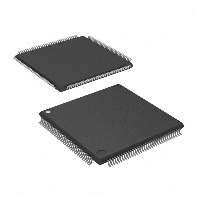
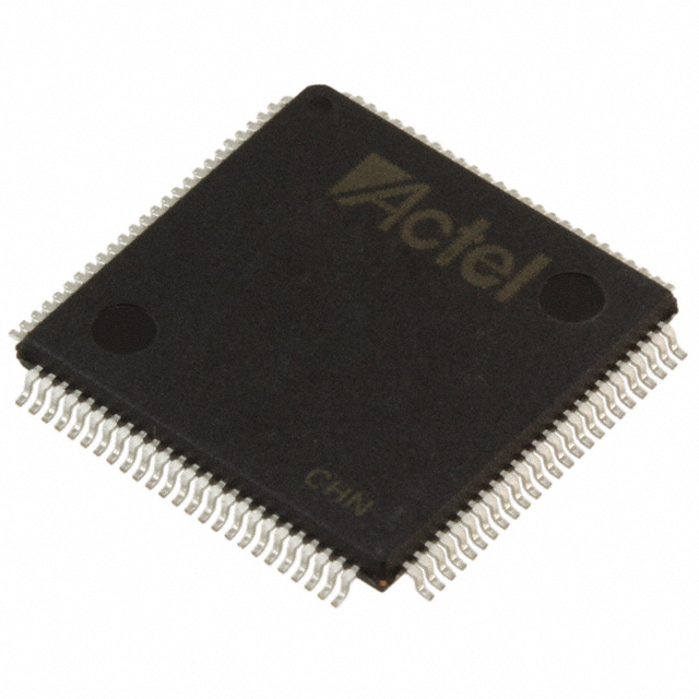
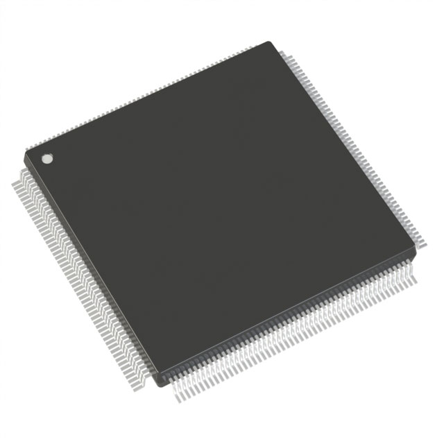
The A54SX32A-2TQ144I is a member of the SX-A family of nonvolatile, single-chip FPGAs. It delivers 48,000 system gates implemented across approximately 2,880 logic elements with 113 user I/Os in a 144-pin thin quad flat pack (TQFP) package.
Designed for industrial-grade embedded applications, the device offers deterministic timing, configurable I/O voltage support, and features intended to simplify system integration and secure in-system programming.
Key Features
- Logic Capacity — Approximately 48,000 system gates realized across about 2,880 logic elements and up to 1,800 dedicated flip-flops for implementing combinational and sequential logic.
- I/O and Packaging — 113 user-programmable I/Os in a 144-TQFP (20×20) package; configurable I/O support for multiple voltage standards enables mixed-voltage interface designs.
- Performance — SX-A family published performance highlights include up to 250 MHz system performance and up to 350 MHz internal performance for timing-critical logic paths.
- Power and Voltage — Wide supply range from 2.25 V to 5.25 V with power-up/power-down friendly behavior that does not require supply sequencing.
- Industrial Temperature Grade — Rated for operation from −40 °C to 85 °C, suitable for industrial environments.
- System Interfaces and Compliance — Hot-swap compliant I/Os and 66 MHz PCI compliance for applications that require PCI signaling and live-board insertion.
- Security and Diagnostics — Includes Actel Secure Programming Technology with FuseLock™ to prevent reverse engineering and supports in-system diagnostic and verification with Silicon Explorer II.
- Test and Reliability — Boundary-scan testing in compliance with IEEE Standard 1149.1 (JTAG) for board-level testability and debug.
- Regulatory — RoHS compliant.
Typical Applications
- Industrial Control and Automation — Deterministic timing, industrial temperature rating, and flexible I/O voltage support make the device suitable for control logic, protocol bridging, and signal conditioning in factory automation systems.
- Embedded Systems — The nonvolatile, single-chip FPGA form factor supports compact embedded designs that need reprogrammable logic and secure in-system updates.
- PCI-Based Systems — With 66 MHz PCI compliance and hot-swap capable I/Os, the device can be used for custom I/O expansion, peripheral interfacing, and board-level logic in PCI environments.
Unique Advantages
- Nonvolatile Single-Chip Solution: Eliminates the need for external configuration memory, simplifying system design and reducing BOM complexity.
- Wide I/O Flexibility: Configurable I/O voltage support (including 5 V tolerance) enables direct interfacing with diverse legacy and modern logic families.
- Industrial Reliability: Specified operation from −40 °C to 85 °C and robust packaging options provide stability for industrial deployments.
- Secure In-System Programming: FuseLock™ programming technology protects intellectual property and supports secure field updates.
- Built-In Testability: IEEE 1149.1 boundary-scan and in-system diagnostic capabilities speed validation, manufacturing test, and field diagnostics.
- Performance Headroom: Family-level internal and system performance figures support timing-critical implementations within the device’s logic capacity.
Why Choose A54SX32A-2TQ144I?
The A54SX32A-2TQ144I combines a substantial logic capacity with flexible, multi-voltage I/O and industrial temperature qualification to address embedded and industrial applications that require secure, reprogrammable logic in a compact TQFP package. Its nonvolatile single-chip architecture and built-in diagnostic and security features reduce system complexity while supporting secure field programmability.
This device is well suited to designers seeking a dependable, industrial-grade FPGA option with deterministic timing, PCI compatibility, and test features that support efficient development and long-term deployment.
Request a quote or submit an inquiry to receive pricing and availability information for the A54SX32A-2TQ144I.


Date Founded: 1989
Headquarters: Chandler, Arizona, USA
Employees: 22,000+
Revenue: $8.349 Billion
Certifications and Memberships: ISO9001:2015, IATF16949:2016, AS 9100D


