
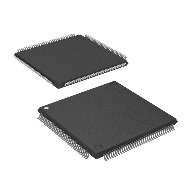
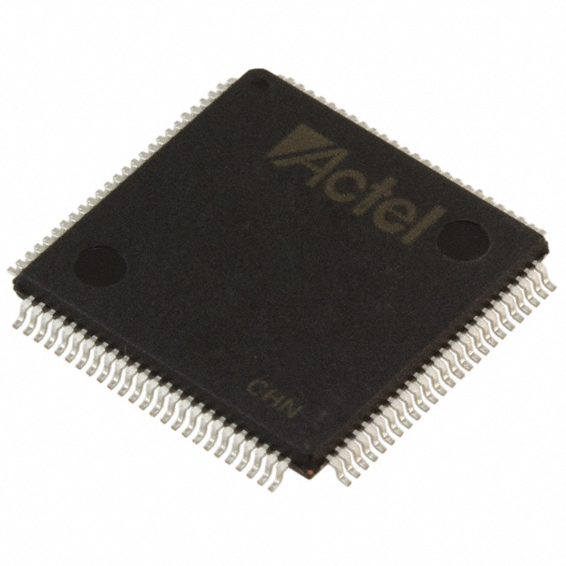
A54SX32A-2TQG144
| Part Description |
SX-A Field Programmable Gate Array (FPGA) IC 113 144-LQFP |
|---|---|
| Quantity | 1,211 Available (as of June 14, 2026) |
| Product Category | Field Programmable Gate Array (FPGA) |
|---|---|
| Manufacturer | Microchip Technology |
| Manufacturing Status | Active |
| Manufacturer Standard Lead Time | 12 Weeks |
| Datasheet |
Specifications & Environmental
| Device Package | 144-TQFP (20x20) | Grade | Commercial | Operating Temperature | 0°C – 70°C | ||
|---|---|---|---|---|---|---|---|
| Package / Case | 144-LQFP | Number of I/O | 113 | Voltage | 2.25 V - 5.25 V | ||
| Mounting Method | Surface Mount | RoHS Compliance | ROHS3 Compliant | REACH Compliance | REACH Unaffected | ||
| Moisture Sensitivity Level | 3 (168 Hours) | Number of LABs/CLBs | 2880 | Number of Logic Elements/Cells | 2880 | ||
| Number of Gates | 48000 | ECCN | 3A991D | HTS Code | 8542.39.0001 | ||
| Qualification | N/A |
Overview of A54SX32A-2TQG144 – SX-A Field Programmable Gate Array (FPGA) IC 113 I/Os, 144-LQFP
The A54SX32A-2TQG144 is a member of the SX-A family of nonvolatile single-chip FPGAs from Microchip Technology. This device delivers 48,000 system gates implemented across 2,880 logic elements with 113 user I/O pins in a 144-pin thin quad flat package (144-LQFP / 144-TQFP). It targets commercial embedded and interface-centric designs that require deterministic timing, flexible I/O voltage support and in-system diagnostic capability.
Key Features
- Core Capacity — 48,000 system gates and approximately 2,880 logic elements provide a mid-range programmable fabric for glue logic, protocol bridging and control functions.
- Programmable Flip-Flops — Family datasheet indicates up to 2,012 dedicated flip-flops are available for state, pipelining and timing control.
- I/O and Voltage Flexibility — 113 user-programmable I/Os on the 144-pin package with configurable I/O support across common signaling levels and mixed-voltage operation (2.5 V, 3.3 V and 5 V) and 5 V input tolerance.
- Performance — SX-A family performance indicators include system performance up to 250 MHz and internal performance up to 350 MHz for timing-critical designs.
- Nonvolatile Single-Chip Solution — Built-in nonvolatile configuration removes the need for external configuration memory and simplifies power-up behavior.
- System Reliability and Test — Boundary-scan testing compliant with IEEE 1149.1 (JTAG) and unique in-system diagnostic/verification capability with Silicon Explorer II (family feature) aid board-level test and verification.
- Power and I/O Controls — Hot-swap compliant I/Os, configurable weak pull-up/pull-down at power-up and individual output slew rate control support robust system integration.
- Package and Mounting — Available in a 144-LQFP / 144-TQFP (20×20) leaded surface-mount package suitable for standard PCB assembly processes.
- Commercial Temperature Grade — Operates from 0 °C to 70 °C and supports a wide supply range from 2.25 V to 5.25 V.
- RoHS Compliance — Device is RoHS compliant.
Typical Applications
- Commercial Embedded Control — Implement glue logic, control state machines and peripheral interfacing where a mid-range programmable fabric is required.
- Interface Bridging and Protocol Conversion — Use the device’s flexible I/O voltage support and deterministic timing for bridging between 3.3 V and 5 V buses or legacy interfaces.
- PCI-Compatible Systems — SX-A family support for 66 MHz PCI signaling and configurable I/O levels make it suitable for PCI-compliant designs that need onboard programmable logic.
- Board-Level Test and In-System Verification — Leverage boundary-scan (IEEE 1149.1) and in-system diagnostic capability to streamline manufacturing test and field diagnostics.
Unique Advantages
- Nonvolatile, single-chip configuration: Eliminates the need for external configuration memory, simplifying BOM and power-up sequencing.
- Flexible mixed-voltage I/O: Support for 2.5 V, 3.3 V and 5 V operation with 5 V tolerance enables direct interfacing with a variety of legacy and modern peripherals.
- Deterministic timing and high internal performance: Family performance metrics (up to 250 MHz system, up to 350 MHz internal) support timing-sensitive logic and high-speed internal paths.
- Built-in testability: IEEE 1149.1 boundary-scan and in-system diagnostics improve board-level debug and manufacturing yield.
- Compact, surface-mount package: 144-LQFP / 144-TQFP packaging offers a balance of pin count and PCB footprint for space-constrained commercial designs.
Why Choose A54SX32A-2TQG144?
The A54SX32A-2TQG144 positions itself as a practical, mid-capacity FPGA option for commercial embedded and interface applications that need nonvolatile configuration, flexible I/O and reliable testability. With 48,000 system gates, roughly 2,880 logic elements and 113 user I/Os in a 144-pin surface-mount package, it is well suited to applications that demand deterministic timing and mixed-voltage connectivity without external configuration components.
Designed for designers seeking a self-contained, testable programmable logic solution, this SX-A family device combines performance-oriented internal timing characteristics with system-level features that simplify integration and board-level verification.
Request a quote or submit an inquiry to receive pricing and availability information for the A54SX32A-2TQG144.


Date Founded: 1989
Headquarters: Chandler, Arizona, USA
Employees: 22,000+
Revenue: $8.349 Billion
Certifications and Memberships: ISO9001:2015, IATF16949:2016, AS 9100D


