
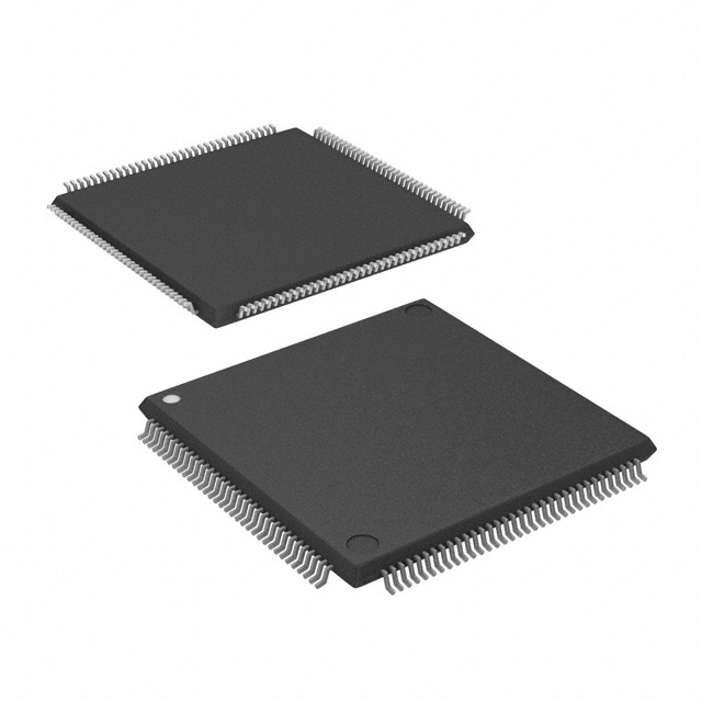
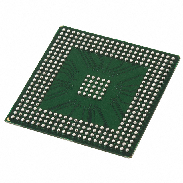
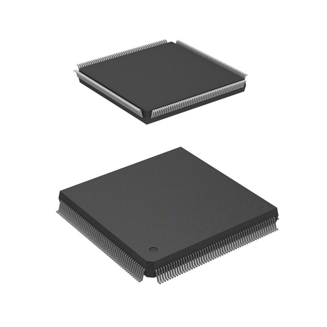
A54SX32A-BG329M
| Part Description |
SX-A Field Programmable Gate Array (FPGA) IC 249 329-BBGA |
|---|---|
| Quantity | 1,687 Available (as of June 17, 2026) |

| Product Category | Field Programmable Gate Array (FPGA) |
|---|---|
| Manufacturer | Microchip Technology |
| Manufacturing Status | Active |
| Manufacturer Standard Lead Time | 20 Weeks |
| Datasheet |
Specifications & Environmental
| Device Package | 329-PBGA (31x31) | Grade | Military | Operating Temperature | -55°C – 125°C | ||
|---|---|---|---|---|---|---|---|
| Package / Case | 329-BBGA | Number of I/O | 249 | Voltage | 2.25 V - 5.25 V | ||
| Mounting Method | Surface Mount | RoHS Compliance | RoHS non-compliant | REACH Compliance | REACH Unaffected | ||
| Moisture Sensitivity Level | 3 (168 Hours) | Number of LABs/CLBs | 2880 | Number of Logic Elements/Cells | 2880 | ||
| Number of Gates | 48000 | ECCN | 3A001A2C | HTS Code | 8542.39.0001 | ||
| Qualification | N/A |
Overview of A54SX32A-BG329M – SX-A Field Programmable Gate Array (FPGA), 249 I/Os, 329-BBGA
The A54SX32A-BG329M is a military-grade SX-A family FPGA in a 329‑ball BGA package, offering a high I/O count and robust operating range for demanding embedded applications. It combines the SX-A family architecture with a nonvolatile, single-chip configuration approach and a broad supply voltage range to support mixed-voltage system designs.
This device targets applications that require high I/O density, deterministic timing and operation across extreme temperatures, leveraging the SX-A family’s performance-oriented features and security capabilities.
Key Features
- Core Capacity Approximately 48,000 system gates and 2,880 logic elements provide a compact, programmable logic fabric for control, glue logic and custom datapaths.
- Performance SX-A family performance characteristics include up to 250 MHz system performance and up to 350 MHz internal performance, enabling high-speed signal processing where required.
- I/O Density & Flexibility 249 user-programmable I/Os support mixed-voltage operation; family-level I/O options include configurable support for 3.3 V/5 V PCI, 5 V TTL, 3.3 V LVTTL and 2.5 V LVCMOS2.
- Nonvolatile Single-Chip Configuration Single-chip, nonvolatile architecture removes the need for external configuration memory and simplifies power-up behavior.
- Security & Test Family features include Actel Secure Programming Technology with FuseLock™ to protect intellectual property and boundary-scan (IEEE 1149.1/JTAG) for board-level testability.
- Robust I/O & System Compatibility Hot-swap compliant I/Os, 66 MHz PCI compliance (family-level) and configurable pull-up/pull-down on I/Os at power-up improve system interoperability and board-level robustness.
- Package & Mounting 329‑BBGA (supplier device package 329‑PBGA, 31 × 31 mm) in a surface-mount package suitable for high-density board designs.
- Power & Environmental Wide supply range from 2.25 V to 5.25 V and military temperature grade with operating range from -55 °C to 125 °C. RoHS compliant.
- Embedded Memory This device lists 0 total on-chip RAM bits; designs should use external memory or internal flip-flop resources as required.
Typical Applications
- Military and Aerospace Systems Military-grade temperature range and packaging make the A54SX32A-BG329M suitable for avionics, ruggedized communications and mission-critical control logic.
- High-Density I/O Gateways High I/O count and configurable I/O standards enable protocol bridging, I/O aggregation and board-level interface consolidation.
- Embedded Control and Signal Processing Logic capacity and family performance characteristics support custom control loops, timing-critical glue logic and moderate-speed signal processing tasks.
- Secure, Nonvolatile FPGA Designs Nonvolatile single-chip configuration and built-in security features allow secure firmware delivery and in-field protection of design IP.
Unique Advantages
- Designed for Harsh Environments: Military-grade temperature range (-55 °C to 125 °C) and BBGA packaging support deployment in extreme-temperature systems.
- High I/O Integration: 249 user I/Os reduce external buffering and simplify board-level routing for multi-interface systems.
- Flexible Voltage Support: Wide supply voltage range (2.25 V–5.25 V) and mixed-voltage I/O capability simplify integration into heterogeneous systems.
- Nonvolatile, Single-Chip Configuration: Eliminates the need for external configuration memory, simplifying BOM and improving system reliability on power cycles.
- Security and Testability: Built-in secure programming technology and boundary-scan support help protect IP and ease production testing.
- Performance Scalability: Family-level performance margins (up to 250 MHz system and 350 MHz internal) let designers target higher-speed internal logic where needed.
Why Choose A54SX32A-BG329M?
The A54SX32A-BG329M brings together the SX-A family’s performance characteristics, nonvolatile single-chip configuration and military-grade robustness in a 329‑ball BGA package. It is well suited for engineers who need a high I/O FPGA with deterministic behavior and secure configuration for demanding embedded and mission-critical applications.
With a wide supply voltage range, high I/O count and family-level features for performance and security, this device offers a compact, resilient solution for long-life designs that require reliable operation across extreme temperatures.
Request a quote or contact sales to check availability, lead times and to discuss how the A54SX32A-BG329M can meet your design requirements.


Date Founded: 1989
Headquarters: Chandler, Arizona, USA
Employees: 22,000+
Revenue: $8.349 Billion
Certifications and Memberships: ISO9001:2015, IATF16949:2016, AS 9100D


