
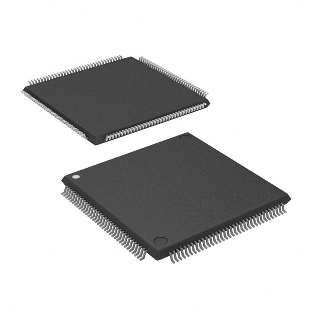
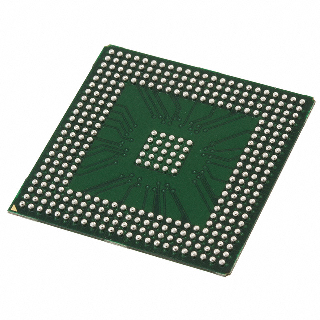
A54SX32A-BG329
| Part Description |
SX-A Field Programmable Gate Array (FPGA) IC 249 329-BBGA |
|---|---|
| Quantity | 540 Available (as of June 15, 2026) |

| Product Category | Field Programmable Gate Array (FPGA) |
|---|---|
| Manufacturer | Microchip Technology |
| Manufacturing Status | Active |
| Manufacturer Standard Lead Time | 20 Weeks |
| Datasheet |
Specifications & Environmental
| Device Package | 329-PBGA (31x31) | Grade | Commercial | Operating Temperature | 0°C – 70°C | ||
|---|---|---|---|---|---|---|---|
| Package / Case | 329-BBGA | Number of I/O | 249 | Voltage | 2.25 V - 5.25 V | ||
| Mounting Method | Surface Mount | RoHS Compliance | RoHS non-compliant | REACH Compliance | REACH Unaffected | ||
| Moisture Sensitivity Level | 3 (168 Hours) | Number of LABs/CLBs | 2880 | Number of Logic Elements/Cells | 2880 | ||
| Number of Gates | 48000 | ECCN | 3A991D | HTS Code | 8542.39.0001 | ||
| Qualification | N/A |
Overview of A54SX32A-BG329 – SX-A Field Programmable Gate Array (FPGA) IC 249 329-BBGA
The A54SX32A-BG329 is a commercial-grade FPGA from Microchip Technology's SX‑A family, delivered as a nonvolatile, single‑chip programmable logic device. It provides 48,000 system gates implemented across 2,880 logic elements with up to 249 user I/O pins in a 329‑ball BGA package.
Designed for commercial embedded applications that require flexible mixed‑voltage I/O and deterministic timing, the device combines high internal performance (up to 350 MHz) and robust system performance (up to 250 MHz) with features such as hot‑swap compliant I/Os, JTAG boundary‑scan, and on‑chip security mechanisms.
Key Features
- Core Capacity: 48,000 system gates realized across 2,880 logic elements, suitable for medium-complexity programmable logic and control functions.
- I/O and Voltage Flexibility: Up to 249 user‑programmable I/O pins with configurable support for multiple voltage standards; device supplies operate from 2.25 V to 5.25 V and support mixed‑voltage operation.
- Performance: Series-level performance targets include up to 250 MHz system performance and up to 350 MHz internal performance for timing‑sensitive logic paths.
- Power-Up and Hot-Swap Friendly: I/O design supports hot‑swap operation and power‑up/down behavior that does not require strict supply sequencing.
- Standards and Test: 66 MHz PCI compliance and IEEE 1149.1 (JTAG) boundary‑scan testing are supported for in‑system testability and legacy bus interfacing.
- Security and Diagnostics: Actel Secure Programming Technology with FuseLock™ for protection against reverse engineering and in‑system diagnostic/verification capability with Silicon Explorer II.
- Package and Mounting: 329‑ball BGA package (product package case: 329‑BBGA; supplier device package listed as 329‑PBGA 31×31) and surface‑mount mounting type.
- Commercial Temperature Grade: Rated for 0 °C to 70 °C operating temperature and RoHS‑compliant packaging.
- Memory: No on‑chip RAM (Total RAM bits: 0), enabling designs that rely on external memory or are optimized for combinational and flip‑flop based logic.
Typical Applications
- Interface Bridging and Glue Logic: Use the A54SX32A-BG329 for board‑level protocol translation and glue logic where mixed‑voltage I/O and configurable pin behavior are required.
- PCI and Peripheral Interfaces: Leverage the device's 66 MHz PCI compliance and 5 V tolerant I/Os for interfacing with PCI‑based subsystems and legacy peripherals.
- Embedded Control and State Machines: Implement control logic, sequencers, and finite state machines using the 2,880 logic elements and dedicated flip‑flop resources.
- In‑System Test and Diagnostics: Integrate boundary‑scan (IEEE 1149.1) and Silicon Explorer II diagnostics for manufacturing test and in‑system verification.
Unique Advantages
- Nonvolatile Single‑Chip Solution: Eliminates external configuration memory and simplifies system boot and configuration management.
- Mixed‑Voltage I/O Flexibility: Supports 2.5 V, 3.3 V, and 5 V operation with 5 V input tolerance and configurable I/O standards, reducing the need for level‑shifters on mixed‑voltage boards.
- Deterministic Timing: User‑controllable timing characteristics help designers achieve predictable timing closure for critical interfaces.
- Security‑Oriented Programming: FuseLock™ technology provides a hardware mechanism to protect designs against reverse engineering and unauthorized access.
- Testability and Diagnostics: Boundary‑scan support plus in‑system diagnostic capability streamline board bring‑up and field troubleshooting.
- Compact, Surface‑Mount BGA Package: 329‑ball BGA footprint enables high I/O density in a compact form factor for board‑space constrained designs.
Why Choose A54SX32A-BG329?
The A54SX32A-BG329 offers a balance of moderate logic capacity, high I/O count, and mixed‑voltage flexibility in a commercial‑grade, nonvolatile FPGA. Its combination of up to 48,000 system gates, 2,880 logic elements, and up to 249 user I/Os makes it well suited for commercial embedded designs that require deterministic timing, in‑system testability, and programmable security.
For teams standardizing on the SX‑A family, the A54SX32A provides a middle‑capacity option that scales within the family while delivering RoHS‑compliant packaging and surface‑mount board integration for production environments.
Request a quote or submit a sourcing inquiry to begin evaluation and procurement of the A54SX32A-BG329 for your next commercial embedded design.


Date Founded: 1989
Headquarters: Chandler, Arizona, USA
Employees: 22,000+
Revenue: $8.349 Billion
Certifications and Memberships: ISO9001:2015, IATF16949:2016, AS 9100D


