
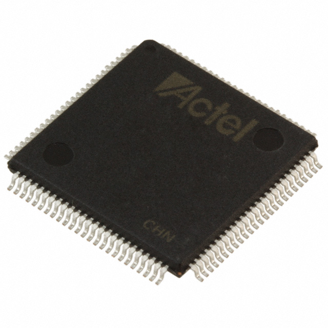
A54SX32A-2TQG144I
| Part Description |
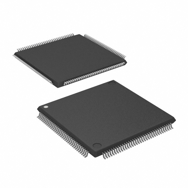
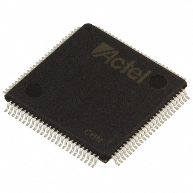
SX-A Field Programmable Gate Array (FPGA) IC 113 144-LQFP |
|---|---|
| Quantity | 136 Available (as of October 7, 2026) |
| Product Category | Field Programmable Gate Array (FPGA) |
|---|---|
| Manufacturer | Microchip Technology |
| Manufacturing Status | Active |
| Manufacturer Standard Lead Time | 12 Weeks |
| Datasheet |
Specifications & Environmental
| Device Package | 144-TQFP (20x20) | Grade | Industrial | Operating Temperature | -40°C – 85°C | ||
|---|---|---|---|---|---|---|---|
| Package / Case | 144-LQFP | Number of I/O | 113 | Voltage | 2.25 V - 5.25 V | ||
| Mounting Method | Surface Mount | RoHS Compliance | ROHS3 Compliant | REACH Compliance | REACH Unaffected | ||
| Moisture Sensitivity Level | 3 (168 Hours) | Number of LABs/CLBs | 2880 | Number of Logic Elements/Cells | 2880 | ||
| Number of Gates | 48000 | ECCN | 3A991D | HTS Code | 8542.39.0001 | ||
| Qualification | N/A |
Overview of A54SX32A-2TQG144I – SX-A Field Programmable Gate Array (FPGA) IC 113 I/Os, 144‑LQFP
The A54SX32A-2TQG144I is an SX-A family FPGA offered in a 144-pin LQFP package. It delivers a nonvolatile, single‑chip FPGA architecture with 48,000 system gates and approximately 2,880 logic elements, targeted for industrial applications requiring reprogrammable logic, mixed‑voltage I/O support and deterministic timing.
With support for a wide supply range (2.25 V to 5.25 V), industrial temperature grading (–40 °C to 85 °C) and 113 user I/Os, this device is suited for embedded control, interface bridging and custom logic roles where robustness and flexible I/O are required.
Key Features
- Core Capacity — 48,000 system gates and 2,880 logic elements provide flexible resources for implementing combinatorial and sequential logic.
- Performance — Documented family performance targets include up to 250 MHz system performance and up to 350 MHz internal performance for time‑critical designs.
- I/O and Voltage Flexibility — 113 user‑programmable I/Os with configurable support for 3.3 V/5 V PCI, 5 V TTL, 3.3 V LVTTL and 2.5 V LVCMOS2; supports mixed‑voltage operation with 5 V input tolerance and 5 V drive strength.
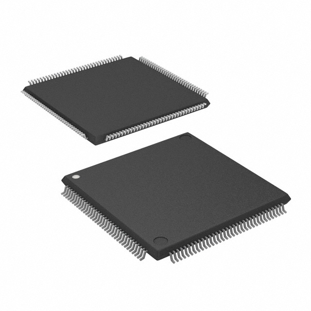
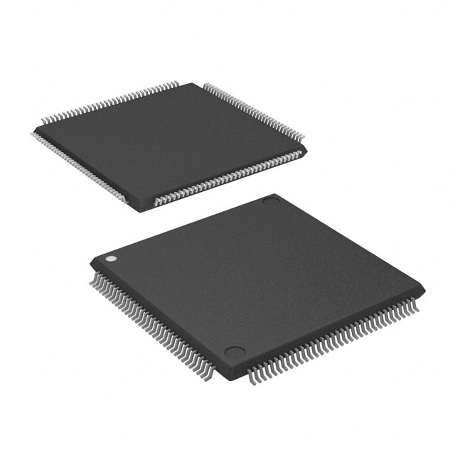
- Package and Mounting — Surface‑mount 144‑pin LQFP (supplier references 144‑TQFP, 20×20) for compact PCB integration.
- Industrial Temperature Grade — Rated for –40 °C to 85 °C operation to meet industrial application environments.
- Power and Reliability — Power‑up/down friendly (no sequencing required for supply voltages) and hot‑swap compliant I/Os to simplify system power management.
- Security and Test — Includes FuseLock™ secure programming technology to protect bitstreams and supports IEEE 1149.1 boundary‑scan (JTAG) for board‑level testability.
- Deterministic Timing and Diagnostics — Family features deterministic, user‑controllable timing and in‑system diagnostic/verification capability.
- Memory — Device reports 0 total RAM bits (no embedded RAM on‑chip).
- Speed Grade — This device is specified with a –2 speed grade (approximately 25% faster than standard, per family ordering information).
Typical Applications
- Industrial control and automation — Use as application‑specific control logic and interface glue in systems that require industrial temperature grading and flexible I/O voltages.
- PCI and legacy bus interfacing — Suitable for PCI‑related logic and bus bridging thanks to 66 MHz PCI compliance and multi‑voltage I/O support.
- Embedded system glue logic — Implement custom peripherals, protocol bridges and timing‑sensitive functions using the device’s logic elements and deterministic timing.
Unique Advantages
- Nonvolatile, single‑chip FPGA — Eliminates the need for external configuration memory, simplifying bill of materials and system startup.
- Flexible mixed‑voltage I/O — Built‑in support for 2.5 V, 3.3 V and 5 V signaling simplifies integration with varied legacy and modern interfaces.
- Industrial temperature rating — Rated operation from –40 °C to 85 °C supports deployment in harsh environments common to industrial systems.
- On‑board security and test support — FuseLock secure programming and IEEE 1149.1 boundary‑scan help protect IP and improve manufacturability.
- Power‑friendly behavior — Power‑up/down friendliness and hot‑swap compliant I/Os reduce system power‑sequencing constraints and support hot‑replace scenarios.
Why Choose A54SX32A-2TQG144I?
The A54SX32A-2TQG144I is positioned as a robust industrial‑grade FPGA option within the SX‑A family, combining a nonvolatile single‑chip architecture with flexible mixed‑voltage I/O and deterministic timing. Its balance of 48,000 system gates, approximately 2,880 logic elements and 113 user I/Os makes it well suited for embedded control, protocol bridging and interface customization where reliable operation across a wide supply range and extended temperature range is required.
Available in a compact 144‑pin LQFP surface‑mount package and featuring integrated security and boundary‑scan testability, this device supports long‑term deployment scenarios that prioritize reprogrammability, board‑level test coverage and simplified system integration.
If you would like pricing, availability or a formal quote for the A54SX32A-2TQG144I, request a quote or submit an inquiry and our team will respond with the requested information.





















Date Founded: 1989
Headquarters: Chandler, Arizona, USA
Employees: 22,000+
Revenue: $8.349 Billion
Certifications and Memberships: ISO9001:2015, IATF16949:2016, AS 9100D




