
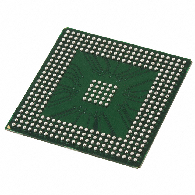
A54SX32A-BGG329
| Part Description |
SX-A Field Programmable Gate Array (FPGA) IC 249 329-BBGA |
|---|---|
| Quantity | 683 Available (as of June 14, 2026) |
| Product Category | Field Programmable Gate Array (FPGA) |
|---|---|
| Manufacturer | Microchip Technology |
| Manufacturing Status | Active |
| Manufacturer Standard Lead Time | 20 Weeks |
| Datasheet |
Specifications & Environmental
| Device Package | 329-PBGA (31x31) | Grade | Commercial | Operating Temperature | 0°C – 70°C | ||
|---|---|---|---|---|---|---|---|
| Package / Case | 329-BBGA | Number of I/O | 249 | Voltage | 2.25 V - 5.25 V | ||
| Mounting Method | Surface Mount | RoHS Compliance | ROHS3 Compliant | REACH Compliance | REACH Unaffected | ||
| Moisture Sensitivity Level | 3 (168 Hours) | Number of LABs/CLBs | 2880 | Number of Logic Elements/Cells | 2880 | ||
| Number of Gates | 48000 | ECCN | 3A991D | HTS Code | 8542.39.0001 | ||
| Qualification | N/A |
Overview of A54SX32A-BGG329 – SX-A Field Programmable Gate Array (FPGA) IC 249 329-BBGA
The A54SX32A-BGG329 is a member of the SX-A family of nonvolatile FPGAs, delivered in a 329-ball BGA package. It provides a programmable logic solution with 48,000 system gates and 2,880 logic elements, supporting up to 249 user I/Os and mixed-voltage operation.
This device targets designs that require on-chip programmability, deterministic timing control, and a high I/O count within a commercial temperature range (0 °C to 70 °C). It supports a wide supply range (2.25 V to 5.25 V) and RoHS-compliant packaging.
Key Features
- Logic Capacity: 48,000 system gates and 2,880 logic elements (cells) to implement complex programmable logic functions.
- User I/O: Up to 249 user-programmable I/O pins, with configurable I/O standards for mixed-voltage operation and 5 V input tolerance.
- Performance: SX-A family performance levels include up to 250 MHz system performance and 350 MHz internal performance as documented for the family.
- Nonvolatile Single-Chip Solution: On-device nonvolatile configuration removes the need for external configuration memory.
- I/O and Bus Support: Hot-swap compliant I/Os and 66 MHz PCI compliance (family-level capability) for peripheral-interface designs.
- Security and Test: Actel Secure Programming Technology with FuseLock for design protection and IEEE 1149.1 (JTAG) boundary-scan testing support.
- Flip-Flops and Registers: Family documentation shows dedicated flip-flop resources; device-level flip-flop capacity supports deterministic, user-controllable timing.
- Package and Mounting: 329-ball plastic BGA (329-PBGA, 31 × 31 mm) surface-mount package suitable for compact board layouts.
- Power and Temperature: Supply range 2.25 V to 5.25 V and commercial operating temperature 0 °C to 70 °C.
- Compliance: RoHS-compliant packaging (G lead-free marking).
Typical Applications
- PCI-compliant peripheral logic: Implement programmable glue logic and interface logic on PCI-based boards using the family’s documented 66 MHz PCI compliance.
- Mixed-voltage system interfaces: Use the device’s configurable I/O and 5 V-tolerant inputs to bridge logic domains and interface legacy TTL/PCI signals.
- In-system diagnostic and verification: Take advantage of the SX-A family in-system diagnostic capabilities and boundary-scan support for board-level testing and verification.
Unique Advantages
- Nonvolatile configuration: Single-chip nonvolatile architecture eliminates external configuration memory and simplifies system power-up behavior.
- High I/O density: 249 user I/Os provide broad connectivity for peripheral interfaces, I/O expansion, and high-pin-count designs.
- Wide supply compatibility: 2.25 V to 5.25 V supply range enables flexible deployment across different logic-voltage domains.
- Security & testability: FuseLock programming technology and IEEE 1149.1 boundary-scan support help protect IP and simplify production test.
- Compact BGA package: 329-ball PBGA (31 × 31 mm) allows a high-pin-count footprint in a compact surface-mount form factor.
- RoHS-compliant: Lead-free packaging supports environmental compliance requirements.
Why Choose A54SX32A-BGG329?
The A54SX32A-BGG329 delivers a balanced combination of programmable logic density, a high I/O count, and family-level performance characteristics that support mixed-voltage interfacing and PCI-compliant designs. Its nonvolatile single-chip configuration, security features, and boundary-scan support simplify system design, firmware management, and production test flows.
This device is well suited for designers who require deterministic timing control, robust I/O flexibility, and a RoHS-compliant BGA package within a commercial temperature range. Its documented family features provide a clear technical foundation for implementing peripheral logic, mixed-voltage interfaces, and in-system verification capabilities.
Request a quote or submit a sales inquiry to obtain pricing, availability, and additional technical information for the A54SX32A-BGG329.


Date Founded: 1989
Headquarters: Chandler, Arizona, USA
Employees: 22,000+
Revenue: $8.349 Billion
Certifications and Memberships: ISO9001:2015, IATF16949:2016, AS 9100D


