
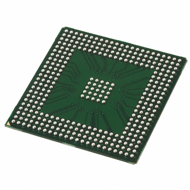
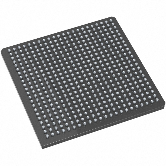
A54SX32A-FBG329
| Part Description |
SX-A Field Programmable Gate Array (FPGA) IC 249 329-BBGA |
|---|---|
| Quantity | 671 Available (as of June 15, 2026) |
| Product Category | Field Programmable Gate Array (FPGA) |
|---|---|
| Manufacturer | Microchip Technology |
| Manufacturing Status | Active |
| Manufacturer Standard Lead Time | 12 Weeks |
| Datasheet |
Specifications & Environmental
| Device Package | 329-PBGA (31x31) | Grade | Commercial | Operating Temperature | 0°C – 70°C | ||
|---|---|---|---|---|---|---|---|
| Package / Case | 329-BBGA | Number of I/O | 249 | Voltage | 2.25 V - 5.25 V | ||
| Mounting Method | Surface Mount | RoHS Compliance | RoHS non-compliant | REACH Compliance | REACH Unaffected | ||
| Moisture Sensitivity Level | 3 (168 Hours) | Number of LABs/CLBs | 2880 | Number of Logic Elements/Cells | 2880 | ||
| Number of Gates | 48000 | ECCN | 3A991D | HTS Code | 8542.39.0001 | ||
| Qualification | N/A |
Overview of A54SX32A-FBG329 – SX-A Field Programmable Gate Array (FPGA) IC 249 329-BBGA
The A54SX32A-FBG329 is a nonvolatile SX-A family FPGA from Microchip Technology designed for commercial electronic designs. It provides a mid-range logic capacity with 48,000 system gates, 2,880 logic elements, and up to 249 user-programmable I/O pins in a 329-ball BGA package.
Built for mixed-voltage interfacing and deterministic timing, this device targets applications that require high I/O density, in-system programmability and on-chip security while operating across a broad supply range and standard commercial temperature conditions.
Key Features
- Logic Capacity — Approximately 48,000 system gates and 2,880 logic elements provide mid-range programmable logic resources for glue logic, control, and interface functions.
- I/O Density — Up to 249 user-programmable I/O pins enable high-density connectivity for complex board-level interfacing.
- Performance — Family-level documented performance includes up to 250 MHz system performance and 350 MHz internal performance for timing-critical paths.
- Nonvolatile Single-Chip Solution — On-chip nonvolatile configuration removes the need for external configuration memory and supports in-system programmability.
- Mixed-Voltage & I/O Flexibility — Configurable I/O supports 2.5 V, 3.3 V and 5 V signaling with 5 V input tolerance and configurable weak pull-up/pull-down on power-up; individual output slew rate control is supported.
- Power Handling — Power-up/power-down friendly design requires no sequencing of supply voltages; operates from a 2.25 V to 5.25 V supply range.
- Standards & Test Support — 66 MHz PCI compliance at the family level and IEEE 1149.1 (JTAG) boundary-scan testing are supported for board-level integration and testability.
- Security & Diagnostics — Actel Secure Programming Technology with FuseLock™ prevents reverse engineering; in-system diagnostic and verification capability is provided via Silicon Explorer II (family feature).
- Package & Mounting — Surface-mount 329-BBGA package (supplier device package: 329-PBGA, 31×31) for compact, high-density PCB designs.
- Temperature & Compliance — Commercial temperature grade (0 °C to 70 °C) and RoHS compliant.
- On-chip Memory — No embedded RAM bits (Total RAM Bits: 0), enabling deterministic usage of flip-flops and logic elements for control and combinatorial functions.
Typical Applications
- Interface bridging and protocol adaptation — High I/O count and configurable I/O voltage support make the device suitable for implementing board-level interface logic and protocol glue, including PCI-class signals at 66 MHz.
- System control and glue logic — The combination of 2,880 logic elements and deterministic timing supports control-state machines, bus arbitration, and other glue logic tasks in commercial electronics.
- In-system programmable designs — Nonvolatile single-chip configuration and in-system diagnostic features enable field updates and verification in deployed equipment.
Unique Advantages
- Nonvolatile, single-chip configuration: Eliminates the need for external configuration memory, simplifying BOM and board layout.
- Flexible mixed-voltage I/O: Configurable support for 2.5 V, 3.3 V and 5 V signaling with 5 V input tolerance reduces the need for level-shifters when interfacing with legacy logic.
- High I/O count in a compact package: 249 user I/Os in a 329-ball BGA enable dense connectivity in space-constrained designs.
- Deterministic, testable implementation: Boundary-scan (JTAG) support and family diagnostic tools help streamline board-level bring-up and in-system validation.
- Security features: FuseLock™ secure programming technology protects design IP and prevents reverse engineering.
- Power sequencing tolerant: Power-up/down friendly operation removes supply sequencing constraints during system power events.
Why Choose A54SX32A-FBG329?
The A54SX32A-FBG329 delivers a balanced mix of logic capacity, high I/O density, and nonvolatile configuration in a commercially graded FPGA package. Its mixed-voltage I/O flexibility, JTAG test support, and on-chip security features make it a practical choice for commercial embedded designs that require reliable, in-system programmable logic and robust board-level interfacing.
This device is well suited for engineers and procurement teams seeking a compact, testable, and secure FPGA solution within the SX-A family for commercial-temperature applications. Its documented family-level performance and configurable I/O options provide clear implementation trade-offs for system designers.
If you would like pricing, availability, or to request a quote for A54SX32A-FBG329, submit an inquiry or request a quote through your preferred purchasing channel.


Date Founded: 1989
Headquarters: Chandler, Arizona, USA
Employees: 22,000+
Revenue: $8.349 Billion
Certifications and Memberships: ISO9001:2015, IATF16949:2016, AS 9100D


