
A54SX32A-CQ84M
| Part Description |
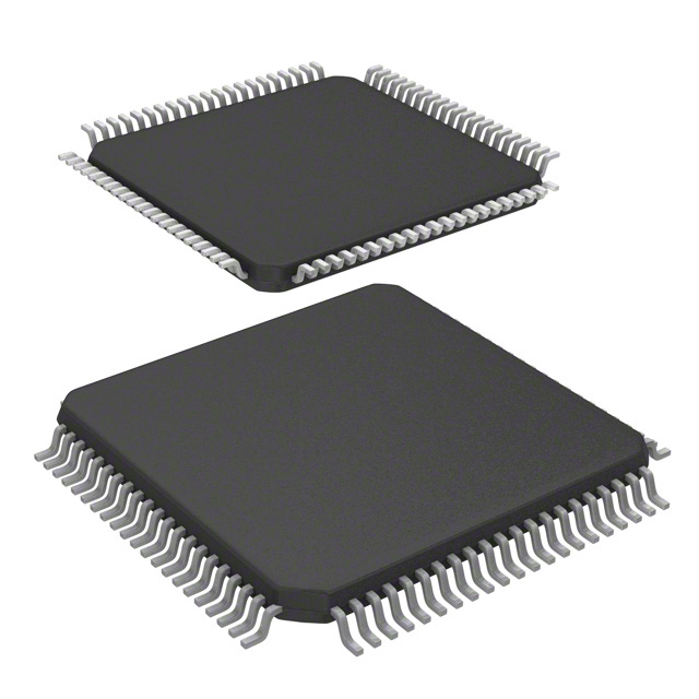
SX-A Field Programmable Gate Array (FPGA) IC 69 84-CQFP Exposed Pad and Tie Bar |
|---|---|
| Quantity | 42 Available (as of June 15, 2026) |

| Product Category | Field Programmable Gate Array (FPGA) |
|---|---|
| Manufacturer | Microchip Technology |
| Manufacturing Status | Active |
| Manufacturer Standard Lead Time | 36 Weeks |
| Datasheet |
Specifications & Environmental
| Device Package | 84-CQFP (42x42) | Grade | Military | Operating Temperature | -55°C – 125°C | ||
|---|---|---|---|---|---|---|---|
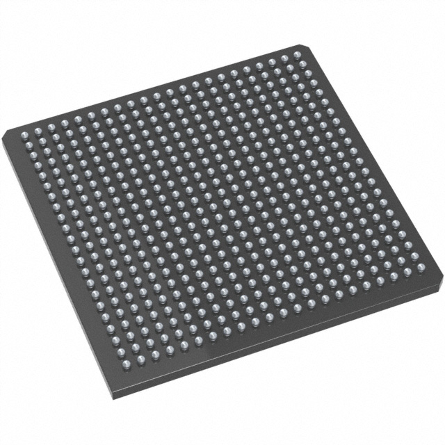
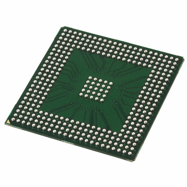
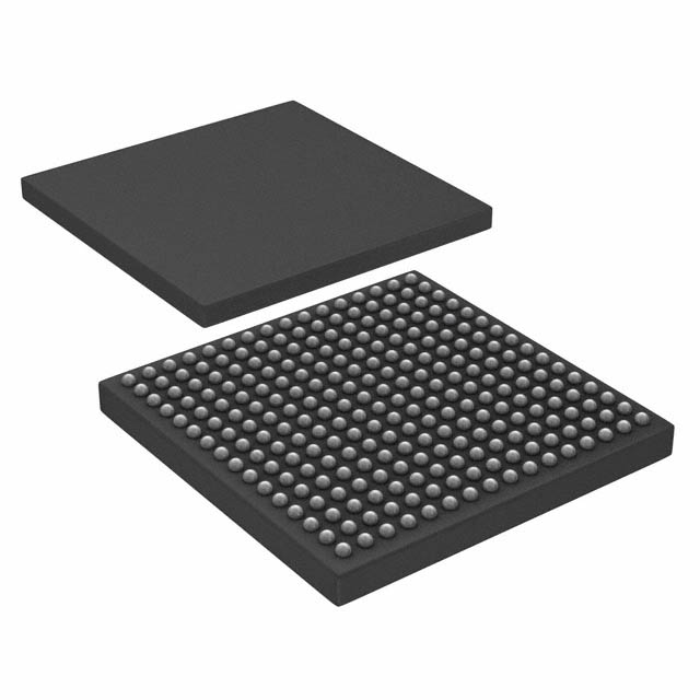
| Package / Case | 84-CQFP Exposed Pad and Tie Bar | Number of I/O | 69 | Voltage | 2.25 V - 5.25 V | ||
| Mounting Method | Surface Mount | RoHS Compliance | RoHS non-compliant | REACH Compliance | REACH Unaffected | ||
| Moisture Sensitivity Level | 3 (168 Hours) | Number of LABs/CLBs | 2880 | Number of Logic Elements/Cells | 2880 | ||
| Number of Gates | 48000 | ECCN | 3A001A2C | HTS Code | 8542.39.0001 | ||
| Qualification | N/A |
Overview of A54SX32A-CQ84M – SX-A Field Programmable Gate Array (FPGA) IC 69 84-CQFP Exposed Pad and Tie Bar
The A54SX32A-CQ84M is a military-grade SX‑A family FPGA from Microchip Technology, offered in an 84-pin ceramic CQFP with exposed pad and tie bar for surface-mount assembly. It delivers deterministic, user-configurable logic resources and I/O flexibility for systems that require high reliability across extreme temperature ranges.
With support for mixed 2.5 V / 3.3 V / 5 V operation and wide supply tolerance, this device is targeted at defense, aerospace and other high-reliability applications that demand secure programmable logic, QML-level qualification, and proven performance under MIL temperature conditions.
Key Features
- Logic Capacity – 48,000 system gates across approximately 2,880 logic elements, providing predictable resource allocation for medium-complexity designs.
- User I/O and Packaging – 69 user I/O pins in an 84‑pin CQFP (42×42) package with exposed pad and tie bar; surface-mount mounting for board-level integration.
- Performance – Up to 215 MHz system performance and 5.3 ns clock‑to‑out (pin‑to‑pin) at military temperature grades, with documented internal performance characteristics.
- Voltage Range – Flexible supply support from 2.25 V to 5.25 V enabling mixed-voltage system interfacing without complex voltage sequencing.
- Military‑Grade Reliability – Qualified for military temperature operation from −55 °C to +125 °C and offered in a QML/Class B flow with MIL-STD-883 screening.
- Secure Programming – Actel Secure Programming Technology (FuseLock) to help protect design IP and prevent reverse engineering.
- System and Test Support – Boundary-scan testing (IEEE 1149.1 / JTAG) and features such as hot‑swap compliant I/Os and power‑up/power‑down friendly behavior to simplify system bring-up and testing.
- Low-Power and Deterministic Timing – Designed for very low power consumption with user-controllable, deterministic timing suitable for time‑sensitive embedded systems.
- RoHS Compliant – Meets RoHS environmental requirements for lead‑free assembly processes.
Typical Applications
- Defense Electronics – Deploys in mission-critical subsystems requiring QML qualification and full military temperature operation for reliable field performance.
- Aerospace Systems – Useful for avionics and flight‑critical control logic where deterministic timing and wide temperature tolerance are essential.
- Secure Embedded Systems – Protects intellectual property and enables secure fielded designs with integrated FuseLock programming technology.
- System Integration and I/O Bridging – Implements custom interface logic and mixed-voltage I/O configurations in compact surface-mount packages.
Unique Advantages
- Military‑Grade Screening: Fabricated and delivered with MIL-STD-883 Class B screening and tested across −55 °C to +125 °C for predictable behavior in harsh environments.
- Secure Device Programming: Includes FuseLock secure programming to reduce risk of reverse engineering and protect design IP in deployed systems.
- Flexible Voltage Support: Operates across 2.25 V–5.25 V supplies and supports mixed 2.5 V/3.3 V/5 V interfacing, reducing the need for level‑shifters.
- Deterministic Performance: Documented clock‑to‑out and internal performance figures support designs that require tight timing control and predictable latency.
- Testability and Integration: Boundary‑scan (JTAG) support, hot‑swap compliant I/Os, and power‑up/down friendly behavior simplify manufacturing test and system integration.
- Compact, Surface‑Mount Ceramic Package: 84‑pin CQFP with exposed pad and tie bar (42×42) provides a compact footprint with robust thermal and mechanical features for high-reliability boards.
Why Choose A54SX32A-CQ84M?
The A54SX32A-CQ84M combines a well-defined logic capacity (48,000 system gates, ~2,880 logic elements) with military-grade qualification, secure programming technology, and a rugged ceramic CQFP package. Its wide supply tolerance and deterministic timing characteristics make it suitable for embedded systems that require dependable logic control and secure, long-term operation in extreme conditions.
Designed for engineers and program managers focused on reliability and IP protection, this FPGA provides an effective balance of integration, predictable performance, and qualification pedigree for defense, aerospace, and other high‑reliability applications.
Request a quote or submit your requirements to receive pricing and availability information for the A54SX32A-CQ84M.


Date Founded: 1989
Headquarters: Chandler, Arizona, USA
Employees: 22,000+
Revenue: $8.349 Billion
Certifications and Memberships: ISO9001:2015, IATF16949:2016, AS 9100D


