
A54SX32A-CQ84
| Part Description |
SX-A Field Programmable Gate Array (FPGA) IC 69 84-CQFP Exposed Pad and Tie Bar |
|---|---|
| Quantity | 404 Available (as of June 15, 2026) |

| Product Category | Field Programmable Gate Array (FPGA) |
|---|---|
| Manufacturer | Microchip Technology |
| Manufacturing Status | Active |
| Manufacturer Standard Lead Time | 36 Weeks |
| Datasheet |
Specifications & Environmental
| Device Package | 84-CQFP (42x42) | Grade | Commercial | Operating Temperature | 0°C – 70°C | ||
|---|---|---|---|---|---|---|---|
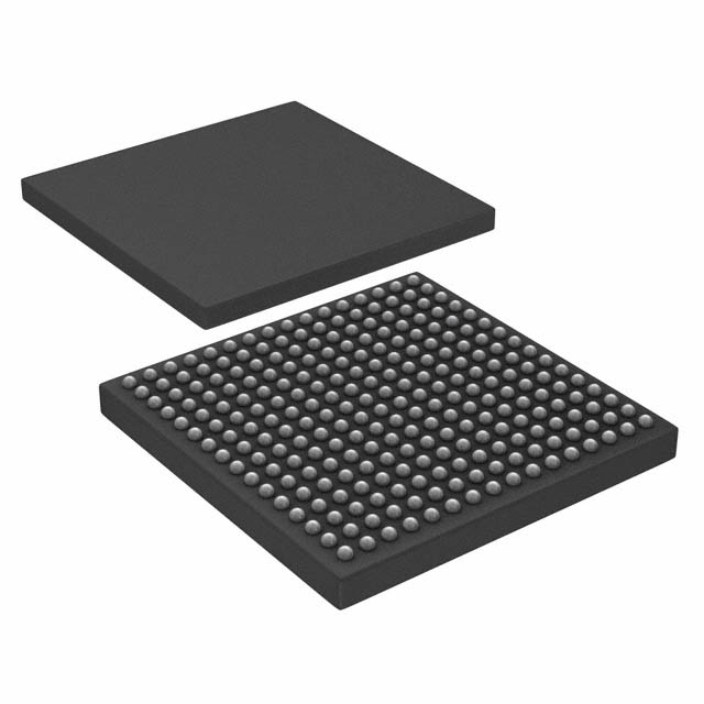
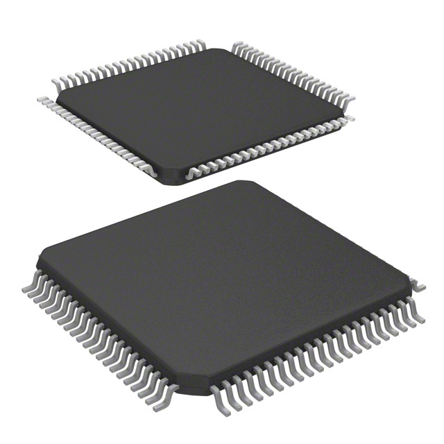
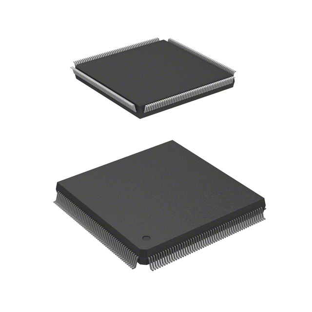
| Package / Case | 84-CQFP Exposed Pad and Tie Bar | Number of I/O | 69 | Voltage | 2.25 V - 5.25 V | ||
| Mounting Method | Surface Mount | RoHS Compliance | RoHS non-compliant | REACH Compliance | REACH Unaffected | ||
| Moisture Sensitivity Level | 3 (168 Hours) | Number of LABs/CLBs | 2880 | Number of Logic Elements/Cells | 2880 | ||
| Number of Gates | 48000 | ECCN | 3A991D | HTS Code | 8542.39.0001 | ||
| Qualification | N/A |
Overview of A54SX32A-CQ84 – SX-A Field Programmable Gate Array (FPGA) IC, 69 I/O, 84-CQFP Exposed Pad
The A54SX32A-CQ84 is a commercial-grade SX-A family field programmable gate array from Microchip Technology designed for surface-mount applications. It delivers a mid-range logic capacity and flexible I/O options in an 84-pin ceramic quad flat pack (CQFP) with exposed pad and tie bar.
Targeted at commercial embedded designs that require configurable logic, mixed-voltage interfacing and compact packaging, the device combines 48,000 system gates and 2,880 logic elements with broad supply voltage support to simplify integration across 2.25 V–5.25 V systems.
Key Features
- Core Capacity — Approximately 48,000 system gates implemented across 2,880 logic elements, providing a balance of logic resources for mid-density designs.
- I/O Count — 69 total I/O pins to support a variety of peripheral interfaces and board-level connectivity requirements.
- No Embedded RAM — Total on-chip RAM bits: 0, suitable for control and glue-logic applications where dedicated external memory is used.
- Package — 84-pin CQFP with exposed pad and tie bar (supplier package: 84-CQFP, 42×42 mm), designed for surface-mount assembly.
- Voltage Range — Flexible supply range from 2.25 V to 5.25 V to accommodate mixed-voltage designs and legacy 5 V interfaces.
- Operating Temperature — Commercial operating range from 0 °C to 70 °C for standard commercial applications.
- Performance — SX-A family timing includes low pin-to-pin clock-to-out values (example: 5.3 ns for A54SX32A in family documentation), enabling responsive logic paths in timing-sensitive applications.
- Power & I/O Behavior — Family-level features include hot-swap–compliant I/Os and power-up/power-down friendliness (no sequencing required for supply voltages), supporting robust board-level power behavior.
- Security & Test — SX-A family capabilities include secure programming technology and IEEE 1149.1 (JTAG) boundary-scan support, enabling design protection and standard test access.
- Compliance — RoHS compliant material status.
Typical Applications
- Commercial Embedded Systems — Implement glue logic, control sequencing and protocol translation where moderate gate density and configurable I/O are required.
- Interface Bridge and Level Translation — Mixed-voltage operation across 2.25 V–5.25 V supports bridging between modern low-voltage logic and legacy 5 V peripherals.
- Board-Level Control and Sequencing — Use the FPGA to centralize board control functions such as reset sequencing, state machines, and peripheral arbitration.
- Prototyping and Low-to-Mid Density Implementations — Compact CQFP packaging and 2,880 logic elements make the device suitable for constrained PCBs and prototype builds requiring reprogrammable logic.
Unique Advantages
- Balanced Logic Capacity: 48,000 system gates and 2,880 logic elements provide sufficient resources for mid-range designs without moving to larger, more costly devices.
- Flexible Voltage Support: 2.25 V–5.25 V supply range enables straightforward integration with a broad set of I/O standards and legacy 5 V systems.
- Compact, Surface-Mount Package: 84-pin CQFP with exposed pad optimizes PCB footprint while providing thermal conduction and mechanical stability.
- Deterministic Timing: Family-level low clock-to-out characteristics support predictable timing closure for control and interface logic.
- Design Protection & Testability: Secure programming technology and JTAG boundary-scan support improve IP protection and manufacturing test access.
- RoHS Compliance: Meets material compliance requirements for modern commercial designs.
Why Choose A54SX32A-CQ84?
The A54SX32A-CQ84 positions itself as a practical, reprogrammable logic solution for commercial embedded applications that need a mid-range mix of gates, predictable timing and flexible I/O voltage support. Its 84-pin CQFP package and exposed pad offer a compact package option for surface-mount assemblies where board space and thermal conduction are considerations.
Designers seeking a reliable, reconfigurable component for glue logic, interface bridging, or control applications will find the A54SX32A-CQ84 a well-rounded option that combines configurable logic density, mixed-voltage operation and family-level features for security and testability.
Request a quote or submit a sourcing inquiry for the A54SX32A-CQ84 to evaluate fit for your next commercial embedded design.


Date Founded: 1989
Headquarters: Chandler, Arizona, USA
Employees: 22,000+
Revenue: $8.349 Billion
Certifications and Memberships: ISO9001:2015, IATF16949:2016, AS 9100D


