
A54SX32A-CQ256
| Part Description |
SX-A Field Programmable Gate Array (FPGA) IC 203 256-BFCQFP with Tie Bar |
|---|---|
| Quantity | 1,378 Available (as of June 15, 2026) |

| Product Category | Field Programmable Gate Array (FPGA) |
|---|---|
| Manufacturer | Microchip Technology |
| Manufacturing Status | Active |
| Manufacturer Standard Lead Time | 38 Weeks |
| Datasheet |
Specifications & Environmental
| Device Package | 256-CQFP (75x75) | Grade | Commercial | Operating Temperature | 0°C – 70°C | ||
|---|---|---|---|---|---|---|---|
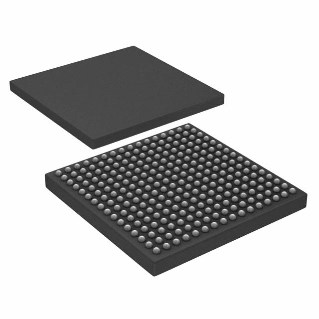
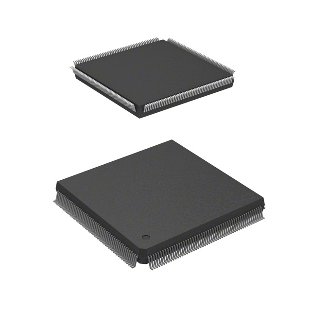
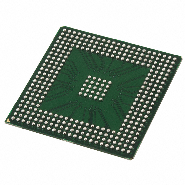
| Package / Case | 256-BFCQFP with Tie Bar | Number of I/O | 203 | Voltage | 2.25 V - 5.25 V | ||
| Mounting Method | Surface Mount | RoHS Compliance | RoHS non-compliant | REACH Compliance | REACH Unaffected | ||
| Moisture Sensitivity Level | 3 (168 Hours) | Number of LABs/CLBs | 2880 | Number of Logic Elements/Cells | 2880 | ||
| Number of Gates | 48000 | ECCN | 3A991D | HTS Code | 8542.39.0001 | ||
| Qualification | N/A |
Overview of A54SX32A-CQ256 – SX-A Field Programmable Gate Array (FPGA) IC 203 256-BFCQFP with Tie Bar
The A54SX32A-CQ256 is a commercial-grade SX‑A family FPGA from Microchip Technology, delivered in a 256‑pin BFCQFP package with tie bar. It provides 48,000 system gates implemented as approximately 2,880 logic elements, with 203 user I/Os for board‑level interfacing and glue logic.
Designed for commercial embedded designs, the device supports a wide supply range (2.25 V to 5.25 V), surface‑mount packaging, and RoHS compliance—making it suitable for mixed‑voltage I/O applications and standard commercial temperature environments (0 °C to 70 °C).
Key Features
- Core Logic — Approximately 48,000 system gates implemented as 2,880 logic elements, enabling mid‑density programmable logic on a single chip.
- Flip‑Flop Resources — Dedicated flip‑flop resources are provided (1,080 maximum per family table entry), supporting register‑based designs and state machines.
- I/O and Voltage — 203 user‑programmable I/O pins with a wide device supply range of 2.25 V to 5.25 V for mixed‑voltage interfacing on a single FPGA.
- Package & Mounting — Supplied in a 256‑BFCQFP package with tie bar (supplier package: 256‑CQFP, 75 × 75), optimized for surface‑mount PCB assembly.
- Temperature & Grade — Commercial grade operation with an ambient temperature range of 0 °C to 70 °C.
- Compliance & Environmental — RoHS‑compliant manufacturing status for regulatory and environmental requirements.
- Family‑Level Capabilities (SX‑A series) — The SX‑A family datasheet documents features such as Actel Secure Programming Technology with FuseLock, boundary‑scan (IEEE 1149.1 JTAG) support, and configurable I/O options for PCI and LVTTL/TTL signaling.
Typical Applications
- PCI and legacy interface logic — Use the SX‑A family’s configurable I/O and documented PCI support to implement board‑level PCI glue logic and interface translation.
- Mixed‑voltage board glue — The wide supply range (2.25 V–5.25 V) and extensive I/O count allow integration of multiple voltage domains and signal standards on a single FPGA.
- Secure, programmable control — Family features such as FuseLock secure programming make the device suitable for designs requiring on‑chip configuration protection.
- Boundary‑scan test environments — IEEE 1149.1 (JTAG) boundary‑scan support simplifies manufacturing test and in‑system diagnostics.
Unique Advantages
- Mid‑density integration: 48,000 system gates and 2,880 logic elements consolidate logic functions that would otherwise require multiple discrete devices.
- Flexible I/O and power: 203 I/Os with a broad 2.25 V–5.25 V supply span enable mixed‑voltage interfacing without external level translators in many cases.
- Commercial temperature ready: Rated for 0 °C to 70 °C operation to match mainstream commercial product requirements.
- Surface‑mount, high‑pin packaging: 256‑pin BFCQFP with tie bar provides high I/O density in a board‑mountable form factor suitable for complex PCB layouts.
- Regulatory and environmental compliance: RoHS compliance supports environmental requirements for commercial products.
Why Choose A54SX32A-CQ256?
The A54SX32A‑CQ256 positions itself as a capable mid‑density FPGA choice for commercial embedded designs that need sizable programmable logic, a high I/O count, and flexible voltage operation. Its 48,000 system gates and 2,880 logic elements deliver the integration and control resources required for interface logic, state machines, and register‑based functions.
Backed by SX‑A family capabilities documented in the product datasheet—such as secure programming options and boundary‑scan support—this device offers a balance of programmability, I/O flexibility, and board‑level packaging that supports sustained product development and production in commercial environments.
Request a quote or submit a parts inquiry to obtain pricing and availability for A54SX32A‑CQ256 and to start your procurement process.


Date Founded: 1989
Headquarters: Chandler, Arizona, USA
Employees: 22,000+
Revenue: $8.349 Billion
Certifications and Memberships: ISO9001:2015, IATF16949:2016, AS 9100D


