
A54SX32A-CQ208M
| Part Description |
SX-A Field Programmable Gate Array (FPGA) IC 174 208-BFCQFP with Tie Bar |
|---|---|
| Quantity | 147 Available (as of June 15, 2026) |

| Product Category | Field Programmable Gate Array (FPGA) |
|---|---|
| Manufacturer | Microchip Technology |
| Manufacturing Status | Active |
| Manufacturer Standard Lead Time | 40 Weeks |
| Datasheet |
Specifications & Environmental
| Device Package | 208-CQFP (75x75) | Grade | Military | Operating Temperature | -55°C – 125°C | ||
|---|---|---|---|---|---|---|---|
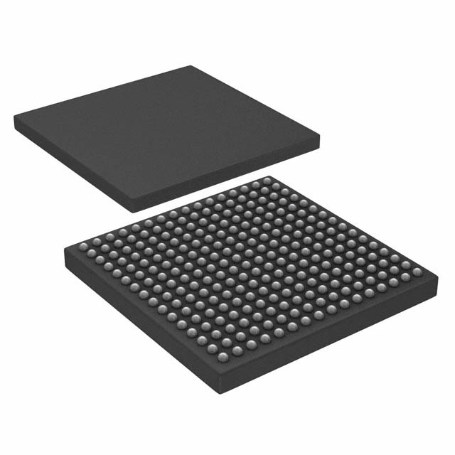
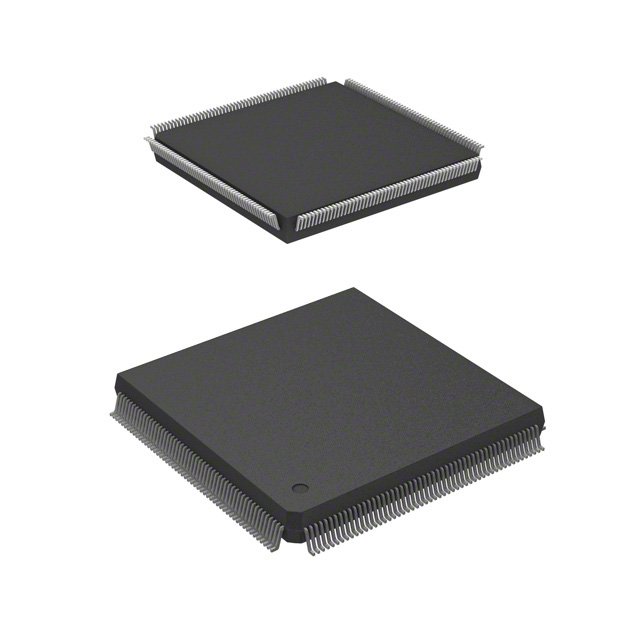
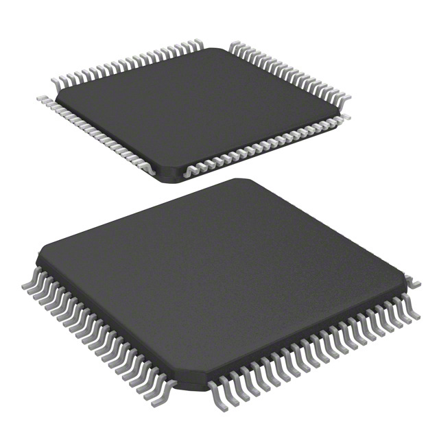
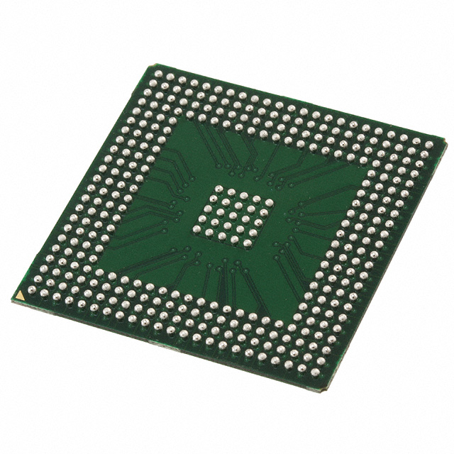
| Package / Case | 208-BFCQFP with Tie Bar | Number of I/O | 174 | Voltage | 2.25 V - 5.25 V | ||
| Mounting Method | Surface Mount | RoHS Compliance | RoHS non-compliant | REACH Compliance | REACH Unaffected | ||
| Moisture Sensitivity Level | 3 (168 Hours) | Number of LABs/CLBs | 2880 | Number of Logic Elements/Cells | 2880 | ||
| Number of Gates | 48000 | ECCN | 3A001A2C | HTS Code | 8542.39.0001 | ||
| Qualification | N/A |
Overview of A54SX32A-CQ208M – SX-A Field Programmable Gate Array (FPGA) IC 174 208-BFCQFP with Tie Bar
The A54SX32A-CQ208M is a military-grade SX-A family FPGA designed for high-reliability embedded systems. It delivers a deterministic programmable fabric with 48,000 system gates, 2,880 logic elements, and 174 user I/O pins in a 208-pin ceramic CQFP package with tie bar.
Engineered for harsh environments, this device supports a wide supply range and full military temperature testing, and includes security and test capabilities suitable for mission-critical and secure applications.
Key Features
- Core & Capacity 48,000 system gates and 2,880 logic elements with up to 1,080 dedicated flip-flops provide a moderate-density programmable fabric for control and glue-logic tasks.
- I/O and Package 174 user-programmable I/Os in a 208-BFCQFP ceramic package with tie bar (supplier package: 208-CQFP, 75×75). Surface-mount mounting type supports standard PCB assembly.
- Voltage and Power Wide supply range from 2.25 V to 5.25 V supports mixed-voltage system integration and flexible interfacing options.
- Temperature and Qualification Military-grade device with operating temperature from −55 °C to +125 °C and QML/MIL qualification flow documented for robust, screened operation.
- Deterministic Timing Family-level timing characteristics include low clock-to-out latency and high internal performance suitable for predictable system timing requirements.
- Security and Reliability Includes Actel Secure Programming Technology with FuseLock to protect design IP and features for power-up/power-down friendly operation without supply sequencing.
- System Test and Integration Boundary-scan (IEEE 1149.1) support and in-system diagnostic/verification capabilities enhance testability and board-level integration.
- Memory No on-chip RAM (Total RAM Bits: 0), enabling deterministic logic-only implementations where embedded RAM is not required.
Typical Applications
- Military & Aerospace Systems High-temperature qualification, QML-class screening, and a −55 °C to +125 °C operating range support avionics and defense electronic subsystems.
- Secure Embedded Controllers On-device FuseLock programming and secure configuration capabilities are suited to applications where IP protection and tamper resistance matter.
- PCI and Legacy Interface Controllers Family-level PCI compliance and configurable I/O voltage support make the device suitable for board-level interface bridging and legacy bus controllers.
- Testable, High-Reliability Designs Boundary-scan support and in-system diagnostics simplify board bring-up, verification, and field maintenance for complex systems.
Unique Advantages
- Military-Grade Screening: Device-level MIL-STD-883 screening and QML-class documentation ensure suitability for screened, high-reliability programs.
- Wide Supply Flexibility: 2.25 V to 5.25 V operation supports mixed-voltage system designs and simplifies interfacing to 2.5 V, 3.3 V, and 5 V domains.
- Secure, Non-Volatile Programming: Actel Secure Programming with FuseLock prevents reverse engineering and helps protect IP in deployed systems.
- Predictable Timing: Family timing characteristics and deterministic behavior support time-critical control and synchronization tasks.
- Board-Level Testability: Boundary-scan and in-system diagnostic capabilities reduce test overhead and improve fault isolation during production and in the field.
- Package and I/O Density: 174 user I/Os in a 208-pin ceramic CQFP provide a balance of I/O routing density and robust package options for space-constrained, rugged boards.
Why Choose A54SX32A-CQ208M?
The A54SX32A-CQ208M combines a deterministic, moderate-density logic fabric with military-grade screening and secure programming features, making it a practical choice for mission-critical embedded designs that require predictable timing, high reliability, and IP protection. Its broad supply range and extensive I/O count simplify interface tasks across mixed-voltage systems.
This device is well suited to systems engineering teams and programs that prioritize long-term robustness, board-level testability, and secure configuration in demanding thermal and environmental conditions.
Request a quote or submit a pricing inquiry for the A54SX32A-CQ208M to evaluate suitability for your next high-reliability FPGA design.


Date Founded: 1989
Headquarters: Chandler, Arizona, USA
Employees: 22,000+
Revenue: $8.349 Billion
Certifications and Memberships: ISO9001:2015, IATF16949:2016, AS 9100D


