
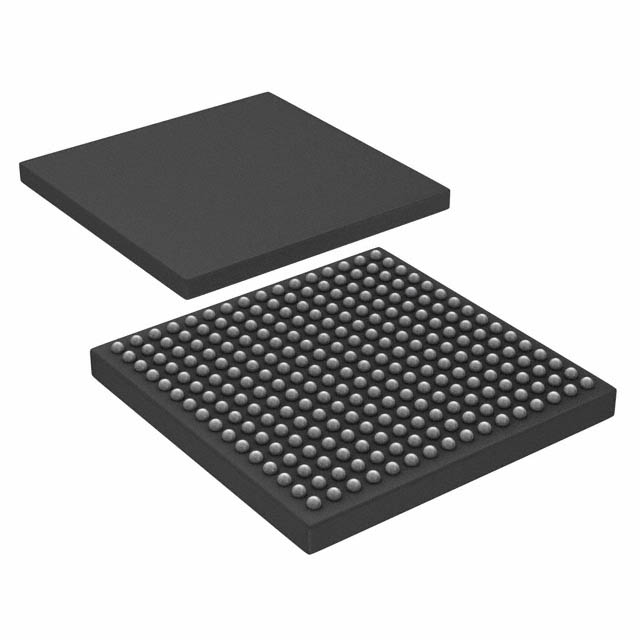
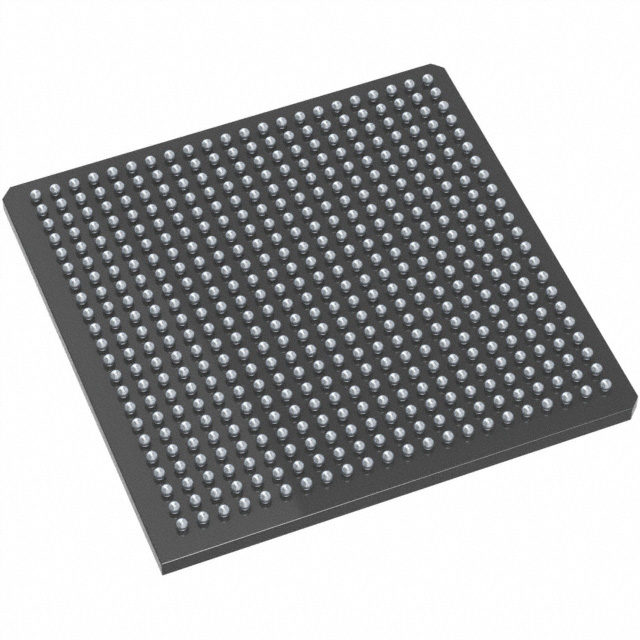
A54SX32A-FG256I
| Part Description |
SX-A Field Programmable Gate Array (FPGA) IC 203 256-BGA |
|---|---|
| Quantity | 1,656 Available (as of June 15, 2026) |
| Product Category | Field Programmable Gate Array (FPGA) |
|---|---|
| Manufacturer | Microchip Technology |
| Manufacturing Status | Active |
| Manufacturer Standard Lead Time | 12 Weeks |
| Datasheet |
Specifications & Environmental
| Device Package | 256-FPBGA (17x17) | Grade | Industrial | Operating Temperature | -40°C – 85°C | ||
|---|---|---|---|---|---|---|---|
| Package / Case | 256-BGA | Number of I/O | 203 | Voltage | 2.25 V - 5.25 V | ||
| Mounting Method | Surface Mount | RoHS Compliance | RoHS non-compliant | REACH Compliance | REACH Unaffected | ||
| Moisture Sensitivity Level | 3 (168 Hours) | Number of LABs/CLBs | 2880 | Number of Logic Elements/Cells | 2880 | ||
| Number of Gates | 48000 | ECCN | 3A991D | HTS Code | 8542.39.0001 | ||
| Qualification | N/A |
Overview of A54SX32A-FG256I – SX-A Field Programmable Gate Array (FPGA) IC 203 256-BGA
The A54SX32A-FG256I is an SX-A family FPGA in a 256-pin fine-pitch BGA package, offering a nonvolatile single-chip FPGA solution targeted at industrial applications. It provides 48,000 system gates and 2,880 logic elements with up to 203 user-programmable I/Os, making it suitable for embedded control, interface, and system-integration roles where mixed-voltage I/O and industrial temperature range support are required.
Designed for deterministic timing and in-system verification, the device combines configurable I/O flexibility and on-chip security features from the SX-A family to support robust, field-updatable FPGA designs.
Key Features
- Logic Capacity — 48,000 system gates and 2,880 logic elements provide substantial programmable logic resources for mid-density designs.
- I/O and Package — 203 user I/Os in a 256-pin fine-pitch BGA (256-FPBGA, 17×17) package for compact board-level integration and high pin-count connectivity.
- Performance (SX-A family) — Series-level performance indicators include up to 250 MHz system performance and up to 350 MHz internal performance (SX-A family data).
- Voltage and Mixed-Voltage I/O — Supply range 2.25 V to 5.25 V with configurable I/O support for multiple signaling levels and 5 V input tolerance (SX-A family characteristics).
- Industrial Temperature Grade — Rated for operation from −40 °C to 85 °C to meet industrial environment requirements.
- Nonvolatile Single-Chip Solution — SX-A family nonvolatile architecture provides single-chip configuration retention and system-level power-up behavior that does not require supply sequencing.
- I/O and System Control Features — Hot-swap compatible I/Os, configurable weak pull-up/pull-down on power-up, and individual output slew rate control (SX-A family).
- System Test and Security — Boundary-scan (IEEE 1149.1) support and Actel Secure Programming Technology with FuseLock for anti-tamper and reverse-engineering protection (SX-A family).
- RoHS Compliant — Device is RoHS compliant.
- On-Chip Memory — Total on-chip RAM bits: 0 (no dedicated embedded RAM).
Typical Applications
- Industrial Control — Use as a programmable logic core for machine control, I/O aggregation, and deterministic timing tasks in industrial systems operating across −40 °C to 85 °C.
- Interface and Bridge Functions — Implement mixed-voltage interface logic and protocol bridging where 203 I/Os and configurable I/O standards are required.
- PCI-Compatible Subsystems — Suitable for subsystem logic in designs that require 66 MHz PCI compliance capabilities (SX-A family feature).
- In-System Diagnostics and Verification — Deploy for systems that benefit from in-system diagnostic capability and boundary-scan testability to simplify validation and service.
Unique Advantages
- Deterministic, User-Controllable Timing: SX-A family timing architecture supports predictable timing closure for time-critical designs.
- Nonvolatile, Single-Chip Configuration: Eliminates external configuration memory and simplifies board-level design and power sequencing.
- Mixed-Voltage I/O with 5 V Tolerance: Broad supply range and configurable I/O options reduce level-shifting components and simplify mixed-voltage system integration.
- Industrial Temperature Qualified: −40 °C to 85 °C rating aligns the device with industrial deployment and harsh-environment operation.
- On-Chip Security Features: FuseLock-based secure programming helps protect intellectual property and prevent reverse engineering (SX-A family).
- Boundary-Scan Testability: IEEE 1149.1-compliant JTAG support enables standardized board-level test and diagnostics.
Why Choose A54SX32A-FG256I?
The A54SX32A-FG256I delivers a balanced combination of mid-level logic capacity, a high I/O count, and industrial-grade temperature support in a compact 256-pin fine-pitch BGA. Its nonvolatile single-chip architecture and configurable mixed-voltage I/Os simplify board design and power management while providing the performance and testability expected from the SX-A family.
This device is well-suited for engineers building industrial embedded systems, interface bridges, and PCI-compatible subsystems who require deterministic timing, in-system verification, and on-chip security in a RoHS-compliant package.
Request a quote or submit an inquiry to obtain pricing, lead time, and availability for the A54SX32A-FG256I. Our team can assist with ordering and technical prerequisites for integration into your design.


Date Founded: 1989
Headquarters: Chandler, Arizona, USA
Employees: 22,000+
Revenue: $8.349 Billion
Certifications and Memberships: ISO9001:2015, IATF16949:2016, AS 9100D


