
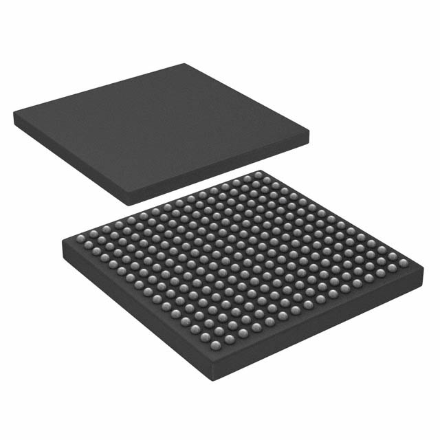
A54SX32A-FGG256
| Part Description |
SX-A Field Programmable Gate Array (FPGA) IC 203 256-BGA |
|---|---|
| Quantity | 1,037 Available (as of June 15, 2026) |

| Product Category | Field Programmable Gate Array (FPGA) |
|---|---|
| Manufacturer | Microchip Technology |
| Manufacturing Status | Active |
| Manufacturer Standard Lead Time | 12 Weeks |
| Datasheet |
Specifications & Environmental
| Device Package | 256-FPBGA (17x17) | Grade | Commercial | Operating Temperature | 0°C – 70°C | ||
|---|---|---|---|---|---|---|---|
| Package / Case | 256-BGA | Number of I/O | 203 | Voltage | 2.25 V - 5.25 V | ||
| Mounting Method | Surface Mount | RoHS Compliance | ROHS3 Compliant | REACH Compliance | REACH Unaffected | ||
| Moisture Sensitivity Level | 3 (168 Hours) | Number of LABs/CLBs | 2880 | Number of Logic Elements/Cells | 2880 | ||
| Number of Gates | 48000 | ECCN | 3A991D | HTS Code | 8542.39.0001 | ||
| Qualification | N/A |
Overview of A54SX32A-FGG256 – SX-A Field Programmable Gate Array (FPGA) IC 203 256-BGA
The A54SX32A-FGG256 is a commercial-grade SX-A family FPGA from Microchip Technology supplied in a 256-ball fine-pitch BGA (17 × 17) package. It delivers a nonvolatile, single-chip FPGA solution with 48,000 system gates (approximately), 2,880 logic elements, and 203 user I/Os—designed for embedded applications that require flexible I/O, secure programming, and deterministic timing.
With support for mixed 2.5 V, 3.3 V and 5 V I/O standards, a wide supply range (2.25 V to 5.25 V), and RoHS-compliant packaging, this device targets designers who need a compact, configurable logic device with on-chip security and in-system diagnostic capabilities.
Key Features
- Core Capacity — Approximately 48,000 system gates and 2,880 logic elements provide mid-range logic density for a range of embedded designs.
- I/O Flexibility — 203 user I/Os with configurable support for 3.3 V/5 V PCI, 5 V TTL, 3.3 V LVTTL and 2.5 V LVCMOS2, plus 5 V input tolerance and 5 V drive strength options.
- Performance — Datasheet-stated performance capability includes up to 250 MHz system performance and up to 350 MHz internal performance for timing-critical functions.
- Nonvolatile Single-Chip Architecture — Device stores configuration on-chip, eliminating the need for external configuration memory.
- Power and I/O Robustness — Hot-swap compliant I/Os and power-up/power-down friendly behavior (no sequencing required for supply voltages) simplify system integration.
- Security and Test — Actel Secure Programming Technology with FuseLock™ for protection against reverse engineering and IEEE 1149.1 (JTAG) boundary-scan testing support.
- Deterministic Timing & Diagnostics — User-controllable timing and in-system diagnostic/verification capability with Silicon Explorer II.
- Package & Mounting — 256-ball fine-pitch FBGA (256-FPBGA, 17 × 17) in a surface-mount format for dense board layouts.
- Power Supply & Temperature — Operating supply range of 2.25 V to 5.25 V; commercial temperature grade rated 0 °C to 70 °C.
- Embedded Memory — No on-chip RAM (Total Ram Bits: 0), enabling predictable, register- and logic-focused designs.
- Regulatory — RoHS-compliant packaging.
Typical Applications
- PCI-based Systems — 66 MHz PCI compliance and configurable 3.3 V/5 V PCI I/O support make the device suitable for legacy and PCI add-on functions.
- Secure or IP-Protected Designs — FuseLock™ secure programming supports designs where protection of bitstreams and IP is required.
- In-System Diagnostics and Verification — Built-in JTAG boundary-scan and Silicon Explorer II support simplify board-level testing and in-field diagnostics.
- Mixed-Voltage Embedded Designs — Configurable I/O voltage support and wide supply range allow interface with 2.5 V, 3.3 V and 5 V peripherals in compact PCB implementations.
Unique Advantages
- Balanced Logic Density: 2,880 logic elements and ~48,000 system gates provide a mid-range capacity for control, glue logic, and protocol handling without excessive board area.
- High I/O Count in a Compact Package: 203 user I/Os in a 256-FPBGA (17 × 17) package enable dense routing and multiple peripheral interfaces in a small footprint.
- On-Chip Nonvolatile Configuration: Single-chip, nonvolatile architecture removes the need for external configuration memory and streamlines system start-up.
- Flexible Voltage and I/O Standards: Support for 2.5 V, 3.3 V and 5 V signaling with 5 V tolerance and drive options helps integrate with a broad set of legacy and modern devices.
- Security and Testability: Integrated FuseLock programming and IEEE 1149.1 boundary-scan improve IP protection and enable standardized board-level testing.
- Design Predictability: Deterministic, user-controllable timing and diagnostic tools assist in timing closure and reduce validation time.
Why Choose A54SX32A-FGG256?
The A54SX32A-FGG256 combines nonvolatile, single-chip FPGA architecture with a mid-range logic capacity and a high I/O count in a compact 256-FPBGA package. Its configurable I/O standards, wide supply voltage range, and built-in security and diagnostic features make it a practical choice for embedded applications that require flexible interfacing, secure configuration, and predictable timing behavior.
This device is suited for design teams seeking a RoHS-compliant, surface-mount FPGA solution for applications such as PCI-interfaced modules, secure logic implementations, and systems that benefit from on-chip configuration and boundary-scan testability.
Request a quote or submit an inquiry to purchase the A54SX32A-FGG256 and evaluate how its configurable I/O, nonvolatile configuration, and on-chip security features fit your next design.


Date Founded: 1989
Headquarters: Chandler, Arizona, USA
Employees: 22,000+
Revenue: $8.349 Billion
Certifications and Memberships: ISO9001:2015, IATF16949:2016, AS 9100D


