
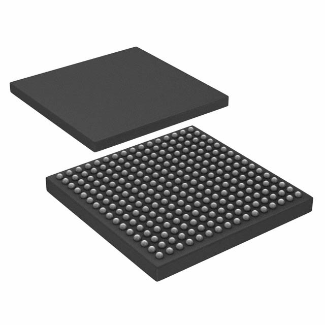
A54SX32A-FG256M
| Part Description |
SX-A Field Programmable Gate Array (FPGA) IC 203 256-BGA |
|---|---|
| Quantity | 901 Available (as of June 18, 2026) |

| Product Category | Field Programmable Gate Array (FPGA) |
|---|---|
| Manufacturer | Microchip Technology |
| Manufacturing Status | Active |
| Manufacturer Standard Lead Time | 20 Weeks |
| Datasheet |
Specifications & Environmental
| Device Package | 256-FPBGA (17x17) | Grade | Military | Operating Temperature | -55°C – 125°C | ||
|---|---|---|---|---|---|---|---|
| Package / Case | 256-BGA | Number of I/O | 203 | Voltage | 2.25 V - 5.25 V | ||
| Mounting Method | Surface Mount | RoHS Compliance | RoHS non-compliant | REACH Compliance | REACH Unaffected | ||
| Moisture Sensitivity Level | 3 (168 Hours) | Number of LABs/CLBs | 2880 | Number of Logic Elements/Cells | 2880 | ||
| Number of Gates | 48000 | ECCN | 3A001A2C | HTS Code | 8542.39.0001 | ||
| Qualification | N/A |
Overview of A54SX32A-FG256M – SX-A Field Programmable Gate Array (FPGA) IC 203 I/O 256-BGA
The A54SX32A-FG256M is a military-grade SX-A family FPGA from Microchip Technology. It delivers a single-chip, nonvolatile FPGA solution with 48,000 system gates and 2,880 logic elements, packaged in a 256-pin fine-pitch BGA suitable for rugged environments.
Designed for applications that require high I/O density, flexible mixed-voltage operation and extended temperature ranges, the device combines configurable I/O support with in-system diagnostic and programming features to simplify implementation in demanding embedded and defense systems.
Key Features
- Logic Capacity — 48,000 system gates and 2,880 logic elements provide mid-range logic integration for control, glue-logic and custom processing functions.
- I/O and Package — 203 user I/Os in a 256-pin fine-pitch BGA (256-FPBGA, 17×17) package for compact, high-density board designs.
- Voltage and I/O Flexibility — Supports mixed-voltage operation (2.5 V, 3.3 V and 5 V) with 5 V input tolerance and 5 V drive strength; supply range 2.25 V to 5.25 V.
- Temperature and Grade — Military grade with operating temperature from −55 °C to 125 °C for high-reliability and harsh-environment deployments.
- Performance — SX-A family performance indicators include up to 250 MHz system performance and up to 350 MHz internal performance (series-level specification).
- Nonvolatile Single-Chip Solution — On-chip nonvolatile configuration avoids external configuration memory and simplifies system start-up.
- I/O and Interface Features — Hot-swap compliant I/Os, configurable support for 3.3 V / 5 V PCI, 5 V TTL, 3.3 V LVTTL and 2.5 V LVCMOS2; configurable pull-up/pull-down on I/O at power-up and individual output slew rate control.
- System Reliability and Test — Boundary-scan testing (IEEE 1149.1 JTAG) and in-system diagnostic/verification capability via Silicon Explorer II (series feature).
- Security — Actel Secure Programming Technology with FuseLock™ provides protection against reverse engineering and design theft (series feature).
- On-Chip Memory — This device reports 0 total RAM bits (no embedded RAM).
Typical Applications
- Military and Defense Electronics — Operation across −55 °C to 125 °C and a military grade package make the device suitable for rugged embedded control and signal-processing subsystems.
- High-Density I/O Control — The 203 available user I/Os in a 256-BGA package support dense interface requirements for board-level glue logic, protocol bridging and custom I/O functions.
- PCI and Mixed-Voltage Interfaces — Configurable I/O levels and PCI support enable use in mixed-voltage interface conversion and legacy PCI-compliant applications.
- Secure In-System Programmable Designs — Nonvolatile, single-chip configuration with FuseLock™ supports applications requiring in-field programmability with design protection.
Unique Advantages
- Military-Grade Reliability: Extended operating temperature and military grade classification reduce risk in harsh-environment designs.
- Single-Chip, Nonvolatile FPGA: Eliminates the need for external configuration memory, simplifying BOM and system boot behavior.
- Flexible I/O Voltage Support: Mixed-voltage operation and 5 V tolerance enable straightforward integration with a wide range of legacy and modern I/O standards.
- High I/O Density in a Compact Package: 203 user I/Os in a 256-FPBGA (17×17) provide a compact solution for high-pin-count requirements.
- Built-In Test and Security: Boundary-scan (JTAG) support and secure programming technology aid manufacturability and IP protection.
- Deterministic Performance: Series-level performance specifications (up to 250 MHz system, 350 MHz internal) support timing-sensitive designs that require predictable behavior.
Why Choose A54SX32A-FG256M?
The A54SX32A-FG256M positions itself as a robust, mid-capacity FPGA option for designs that demand military-grade operation, high I/O count and nonvolatile in-system programmability. Its combination of 48,000 system gates, 2,880 logic elements, configurable mixed-voltage I/O and secure programming makes it well suited to aerospace, defense and other high-reliability embedded systems.
Selecting this Microchip Technology FPGA helps teams consolidate logic into a single nonvolatile device, simplify board-level design with flexible I/O support, and maintain testability and IP protection through JTAG and FuseLock™ technologies—delivering a practical balance of integration, configurability and ruggedness.
Request a quote or submit a pricing inquiry for the A54SX32A-FG256M to get availability and procurement details for your project needs.


Date Founded: 1989
Headquarters: Chandler, Arizona, USA
Employees: 22,000+
Revenue: $8.349 Billion
Certifications and Memberships: ISO9001:2015, IATF16949:2016, AS 9100D


