
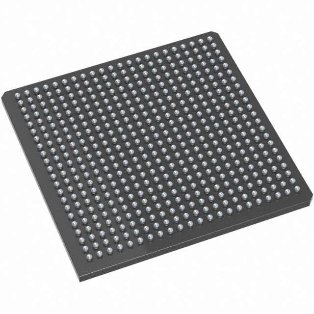
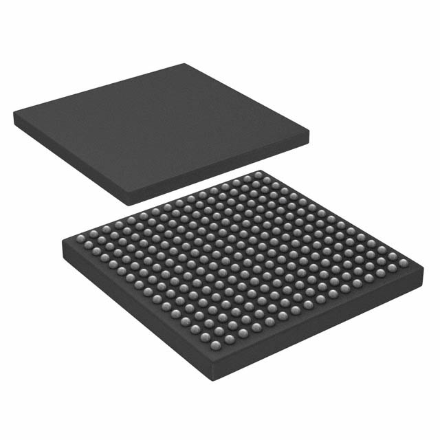
A54SX32A-FG484
| Part Description |
SX-A Field Programmable Gate Array (FPGA) IC 249 484-BGA |
|---|---|
| Quantity | 960 Available (as of June 16, 2026) |
| Product Category | Field Programmable Gate Array (FPGA) |
|---|---|
| Manufacturer | Microchip Technology |
| Manufacturing Status | Active |
| Manufacturer Standard Lead Time | 52 Weeks |
| Datasheet |
Specifications & Environmental
| Device Package | 484-FPBGA (27X27) | Grade | Commercial | Operating Temperature | 0°C – 70°C | ||
|---|---|---|---|---|---|---|---|
| Package / Case | 484-BGA | Number of I/O | 249 | Voltage | 2.25 V - 5.25 V | ||
| Mounting Method | Surface Mount | RoHS Compliance | RoHS non-compliant | REACH Compliance | REACH Unaffected | ||
| Moisture Sensitivity Level | 3 (168 Hours) | Number of LABs/CLBs | 2880 | Number of Logic Elements/Cells | 2880 | ||
| Number of Gates | 48000 | ECCN | 3A991D | HTS Code | 8542.39.0001 | ||
| Qualification | N/A |
Overview of A54SX32A-FG484 – SX-A Field Programmable Gate Array (FPGA) IC 249 484-BGA
The A54SX32A-FG484 is a member of the SX-A family of nonvolatile FPGAs from Microchip Technology. This device provides 48,000 system gates implemented as 2,880 logic elements with up to 249 user‑programmable I/O pins in a 484‑ball fine‑pitch BGA package.
Designed for commercial embedded applications, the A54SX32A-FG484 supports mixed‑voltage I/O and high system performance (250 MHz system, 350 MHz internal) while offering single‑chip, nonvolatile configuration and on‑chip security options to protect intellectual property.
Key Features
- Logic Capacity — 48,000 system gates implemented as 2,880 logic elements (combinatorial cells and registers) to support moderate complexity digital designs.
- High Performance — Documented system performance up to 250 MHz and internal performance up to 350 MHz for timing‑sensitive logic paths.
- I/O Flexibility — 249 user I/Os with configurable support for 3.3 V/5 V PCI, 5 V TTL, 3.3 V LVTTL and 2.5 V LVCMOS2; 5 V input tolerance and 5 V drive strength are supported as specified in the family datasheet.
- Nonvolatile Single‑Chip Configuration — Single‑chip, nonvolatile architecture eliminates the need for external configuration memory and preserves configuration across power cycles.
- Power and I/O Safety — Hot‑swap compliant I/Os and power‑up/power‑down friendly operation with no supply sequencing required per the SX‑A family documentation.
- Security and Testability — Actel Secure Programming Technology (FuseLock™) to guard against reverse engineering and boundary‑scan testing compliant with IEEE 1149.1 (JTAG) for board‑level diagnostics.
- Package and Mounting — 484‑ball Fine‑Pitch BGA (484‑FPBGA, 27×27 mm) in a surface‑mount form factor; RoHS compliant packaging available.
- Voltage and Temperature — Supply voltage range 2.25 V to 5.25 V and commercial operating temperature 0 °C to 70 °C as specified for this part number.
- Clocking — Device supports three global clocks as defined for the A54SX32A in the SX‑A family documentation.
- Resource Utilization — Family documentation notes support for up to 100% resource utilization and 100% pin locking for deterministic designs.
- On‑chip RAM — Total on‑chip RAM reported as 0 bits for this device (no embedded RAM).
Typical Applications
- Commercial Embedded Systems — Single‑chip nonvolatile FPGA with flexible I/O and mixed‑voltage support for consumer and commercial embedded control and interface tasks.
- I/O‑Intensive Peripheral Interfaces — High I/O count (249 pins) and 5 V tolerance enable bridging and interfacing to legacy peripherals, sensors, and external logic.
- PCI and Bus Bridging — SX‑A family documentation lists 66 MHz PCI compliance and configurable 3.3 V/5 V PCI I/O support suited to legacy bus interface implementations.
- In‑System Diagnostics and Verification — Built‑in support for in‑system diagnostic and verification via Silicon Explorer II as referenced in the SX‑A family documentation.
Unique Advantages
- Nonvolatile Single‑Chip Configuration: Eliminates external configuration components and simplifies BOM and board design.
- Mixed‑Voltage I/O with 5 V Tolerance: Reduces the need for level‑shifters when interfacing with diverse peripheral voltage domains.
- Security‑Oriented Programming: FuseLock™ programming technology protects design IP against reverse engineering.
- Power‑Friendly I/Os: Hot‑swap compliance and power‑up/power‑down friendly behavior simplify system power sequencing.
- Deterministic Timing and Full Resource Utilization: Family features support deterministic, user‑controllable timing and high resource utilization for tight design control.
- Commercial Temperature Optimization: Designed and specified for commercial temperature operation (0 °C to 70 °C) for mainstream electronics applications.
Why Choose A54SX32A-FG484?
The A54SX32A-FG484 balances moderate logic capacity and high I/O density in a single, nonvolatile FPGA package suitable for commercial embedded designs that require mixed‑voltage interfacing and configuration retention without external memory. Its combination of deterministic timing features, hot‑swap I/Os, and security programming options provides designers with a compact, integrated solution for I/O‑heavy applications and legacy interface bridging.
This device is appropriate for engineering teams seeking a single‑chip FPGA with established SX‑A family features, straightforward power behavior, and support for in‑system diagnostics and boundary‑scan testing to simplify bring‑up and validation.
Request a quote or contact sales to check pricing and availability for the A54SX32A-FG484 and to discuss how this FPGA can fit your next commercial embedded design.


Date Founded: 1989
Headquarters: Chandler, Arizona, USA
Employees: 22,000+
Revenue: $8.349 Billion
Certifications and Memberships: ISO9001:2015, IATF16949:2016, AS 9100D


