
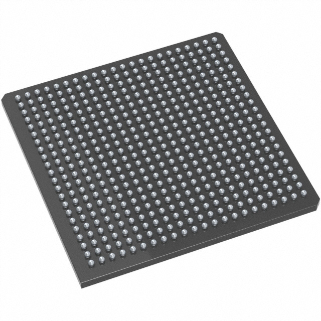
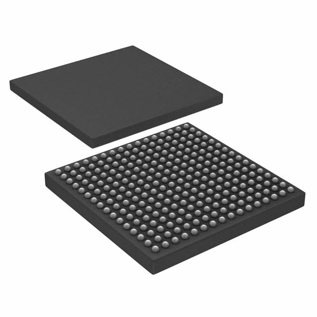
A54SX72A-FFGG484
| Part Description |
SX-A Field Programmable Gate Array (FPGA) IC 360 484-BGA |
|---|---|
| Quantity | 500 Available (as of June 19, 2026) |
| Product Category | Field Programmable Gate Array (FPGA) |
|---|---|
| Manufacturer | Microchip Technology |
| Manufacturing Status | Active |
| Manufacturer Standard Lead Time | 12 Weeks |
| Datasheet |
Specifications & Environmental
| Device Package | 484-FPBGA (27X27) | Grade | Commercial | Operating Temperature | 0°C – 70°C | ||
|---|---|---|---|---|---|---|---|
| Package / Case | 484-BGA | Number of I/O | 360 | Voltage | 2.25 V - 5.25 V | ||
| Mounting Method | Surface Mount | RoHS Compliance | ROHS3 Compliant | REACH Compliance | REACH Unaffected | ||
| Moisture Sensitivity Level | 3 (168 Hours) | Number of LABs/CLBs | 6036 | Number of Logic Elements/Cells | 6036 | ||
| Number of Gates | 108000 | ECCN | 3A991D | HTS Code | 8542.39.0001 | ||
| Qualification | N/A |
Overview of A54SX72A-FFGG484 – SX-A Field Programmable Gate Array (FPGA) IC 360 484-BGA
The A54SX72A-FFGG484 is a commercial-grade, nonvolatile SX-A family FPGA provided in a 484-ball fine-pitch BGA package. It combines a high I/O count and substantial logic capacity with mixed-voltage I/O support and built-in security and diagnostic features.
Designed for commercial embedded designs that require deterministic timing, flexible I/O configuration, and onboard nonvolatile configuration, this device addresses use cases such as PCI interfacing, in-system verification, and mixed-voltage system integration.
Key Features
- Logic Capacity 6,036 logic elements delivering up to 108,000 system gates and up to 2,012 dedicated flip-flops for complex combinational and sequential logic.
- I/O Density & Flexibility Up to 360 user-programmable I/O pins with configurable support for 3.3 V / 5 V PCI, 5 V TTL, 3.3 V LVTTL and 2.5 V LVCMOS2 signaling. I/Os are hot-swap compliant and support 5 V input tolerance and 5 V drive strength.
- Performance System performance up to 250 MHz and internal performance up to 350 MHz as specified for the SX-A family.
- Power & Reliability Power-up/down friendly design with no sequencing required for supply voltages, configurable weak pull-up or pull-down on I/O at power-up, and individual output slew-rate control.
- Security & Diagnostics Nonvolatile single-chip configuration with Actel Secure Programming Technology (FuseLock™) to protect design IP, plus in-system diagnostic and verification capability via Silicon Explorer II and IEEE 1149.1 (JTAG) boundary-scan support.
- Package & Environmental 484-ball fine-pitch BGA (484-FPBGA, 27×27) surface-mount package; commercial operating temperature range 0 °C to 70 °C; RoHS compliant.
- Voltage Range Flexible supply operation from 2.25 V to 5.25 V to support mixed-voltage system architectures.
Typical Applications
- PCI and Legacy Interface Bridging Use the device’s PCI-compliant I/O and mixed-voltage support to implement interface bridging and legacy peripheral support in commercial systems.
- Embedded Control and Prototyping High logic capacity and up to 360 I/Os make it suitable for embedded control, prototyping of complex logic, and custom peripheral aggregation.
- Secure IP Implementation FuseLock™ secure programming and on-chip nonvolatile configuration help protect proprietary logic and firmware in commercial products.
- In-System Test and Verification Built-in JTAG boundary-scan and Silicon Explorer II diagnostic capability simplifies manufacturing test and field verification.
Unique Advantages
- High I/O Count for Dense Designs: 360 user-programmable I/Os enable dense peripheral and bus interfaces without external multiplexing.
- Nonvolatile Single-Chip Solution: Eliminates the need for external configuration memory, simplifying BOM and board design.
- Configurable Mixed-Voltage I/O: Support for multiple I/O standards and 5 V tolerance aids integration into mixed-voltage systems.
- Deterministic Timing Control: Architecture features that support deterministic, user-controllable timing for predictable system behavior.
- Integrated IP Protection: FuseLock™ secure programming technology provides a hardware-level barrier against reverse engineering.
- Commercial Temperature Range: Rated for 0 °C to 70 °C for deployments in standard commercial environments.
Why Choose A54SX72A-FFGG484?
The A54SX72A-FFGG484 delivers a balanced combination of logic capacity, high I/O density, and mixed-voltage flexibility in a single nonvolatile FPGA. Its SX-A family features—deterministic timing, in-system diagnostics, and secure programming—make it well suited for commercial embedded designs that require reliable configuration retention and secure IP protection.
Choose this device when you need a commercial-grade FPGA that simplifies board-level design (single-chip configuration), supports a wide range of I/O standards, and provides integrated test and security features to shorten development and manufacturing cycles.
Request a quote or contact sales to discuss availability, pricing, and how the A54SX72A-FFGG484 can fit your next commercial FPGA design.


Date Founded: 1989
Headquarters: Chandler, Arizona, USA
Employees: 22,000+
Revenue: $8.349 Billion
Certifications and Memberships: ISO9001:2015, IATF16949:2016, AS 9100D


