
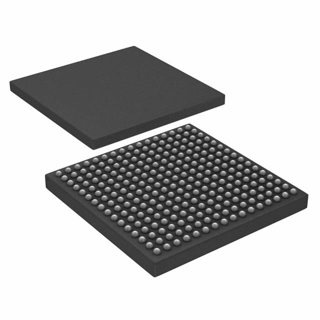
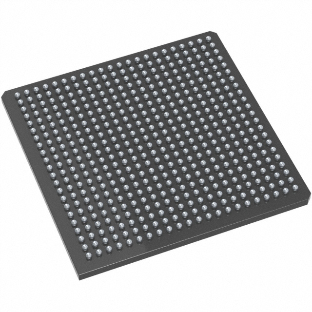
A54SX72A-FG256
| Part Description |
SX-A Field Programmable Gate Array (FPGA) IC 203 256-BGA |
|---|---|
| Quantity | 160 Available (as of June 14, 2026) |

| Product Category | Field Programmable Gate Array (FPGA) |
|---|---|
| Manufacturer | Microchip Technology |
| Manufacturing Status | Active |
| Manufacturer Standard Lead Time | 12 Weeks |
| Datasheet |
Specifications & Environmental
| Device Package | 256-FPBGA (17x17) | Grade | Commercial | Operating Temperature | 0°C – 70°C | ||
|---|---|---|---|---|---|---|---|
| Package / Case | 256-BGA | Number of I/O | 203 | Voltage | 2.25 V - 5.25 V | ||
| Mounting Method | Surface Mount | RoHS Compliance | RoHS non-compliant | REACH Compliance | REACH Unaffected | ||
| Moisture Sensitivity Level | 3 (168 Hours) | Number of LABs/CLBs | 6036 | Number of Logic Elements/Cells | 6036 | ||
| Number of Gates | 108000 | ECCN | 3A991D | HTS Code | 8542.39.0001 | ||
| Qualification | N/A |
Overview of A54SX72A-FG256 – SX-A Field Programmable Gate Array (FPGA) IC 203 256-BGA
The A54SX72A-FG256 is a commercial-grade SX-A family FPGA from Microchip Technology offered in a 256-ball fine-pitch BGA (256-FPBGA, 17×17) package. It provides a nonvolatile, single-chip programmable logic solution with 108,000 system gates and 6,036 logic elements for board-level control, interface bridging, and embedded system functions.
Designed for mixed-voltage systems, the device supports a wide supply range (2.25 V to 5.25 V) and up to 203 user I/Os, delivering deterministic timing, in-system diagnostic capability, and security features suited to a variety of commercial electronic designs.
Key Features
- Logic Capacity 6,036 logic elements and approximately 108,000 system gates to implement medium-density FPGA functions.
- Flip-Flops and Clocks Up to 2,012 dedicated flip-flops with 3 global clocks and 4 quadrant clocks for structured clocking domains.
- High-Speed Performance SX-A family performance characteristics include up to 250 MHz system performance and 350 MHz internal performance as documented for the family.
- I/O Density and Flexibility 203 user I/Os with configurable I/O support for multiple standards, enabling mixed-voltage operation and flexible interfacing.
- Mixed-Voltage and 5 V Tolerance Supports 2.5 V, 3.3 V, and 5 V mixed-voltage operation with 5 V input tolerance and 5 V drive strength where applicable.
- Nonvolatile Single-Chip Configuration Nonvolatile architecture provides single-chip configuration without external configuration memory.
- Design Security and Test Includes Actel Secure Programming Technology (FuseLock™) to protect design IP and supports IEEE 1149.1 JTAG boundary-scan testing plus in-system diagnostic and verification via Silicon Explorer II.
- Package and Mounting 256-FPBGA (17×17) fine-pitch BGA, surface-mount package optimized for compact board designs; RoHS compliant.
- Supply and Operating Range Wide supply range of 2.25 V to 5.25 V and commercial operating temperature 0 °C to 70 °C.
- Board-Friendly I/Os Hot-swap compliant I/Os and configurable weak pull-up/pull-down options help simplify system power sequencing and hot-insert scenarios.
Typical Applications
- Interface Bridging and Glue Logic Use the A54SX72A-FG256 to implement board-level protocol bridging and custom interface logic where mixed-voltage I/O and deterministic timing are required.
- PCI-Compatible Systems Suitable for designs that require 66 MHz PCI compatibility and flexible I/O standards for legacy or mixed-voltage PCI signaling.
- Secure or IP-Sensitive Designs Applications that require on-chip IP protection and in-system verification can leverage the device’s FuseLock security and diagnostic capabilities.
- In-System Configurable Control Field-programmable control logic, state machines, and peripheral management functions that benefit from nonvolatile, single-chip configuration.
Unique Advantages
- Nonvolatile, single-chip solution: Eliminates the need for external configuration memory, simplifying BOM and system design.
- Robust I/O flexibility: Configurable I/O standards and mixed-voltage support (2.5 V, 3.3 V, 5 V) with 5 V tolerance enable versatile interfacing without extra level shifting in many use cases.
- Security and test built in: FuseLock™ secure programming and IEEE 1149.1 boundary-scan plus in-system diagnostics provide IP protection and easier production testability.
- Balanced capacity and performance: 6,036 logic elements, ~108,000 system gates, and family-documented performance figures support medium-density designs that need predictable timing.
- Compact BGA package: 256-FPBGA (17×17) fine-pitch BGA delivers high I/O count (203 pins) in a compact surface-mount footprint.
- Commercial readiness: Commercial-grade temperature range (0 °C to 70 °C) and RoHS compliance for standard commercial applications.
Why Choose A54SX72A-FG256?
The A54SX72A-FG256 provides a balanced combination of logic capacity, flexible I/O, and nonvolatile single-chip configuration for commercial embedded designs. Its documented family-level performance, on-chip security features, and diagnostic support make it a practical choice for designers needing medium-density programmable logic with predictable behavior and simplified system integration.
This device is well suited to engineers building board-level interface logic, PCI-compatible subsystems, and secure programmable control functions who require a compact, RoHS-compliant BGA package with mixed-voltage I/O capabilities.
Request a quote or submit an inquiry to receive pricing and availability information for the A54SX72A-FG256. Provide your requirements and quantity to expedite response.


Date Founded: 1989
Headquarters: Chandler, Arizona, USA
Employees: 22,000+
Revenue: $8.349 Billion
Certifications and Memberships: ISO9001:2015, IATF16949:2016, AS 9100D


