
A54SX72A-FFG256
| Part Description |
SX-A Field Programmable Gate Array (FPGA) IC 203 256-BGA |
|---|---|
| Quantity | 1,157 Available (as of June 10, 2026) |

| Product Category | Field Programmable Gate Array (FPGA) |
|---|---|
| Manufacturer | Microchip Technology |
| Manufacturing Status | Active |
| Manufacturer Standard Lead Time | 12 Weeks |
| Datasheet |
Specifications & Environmental
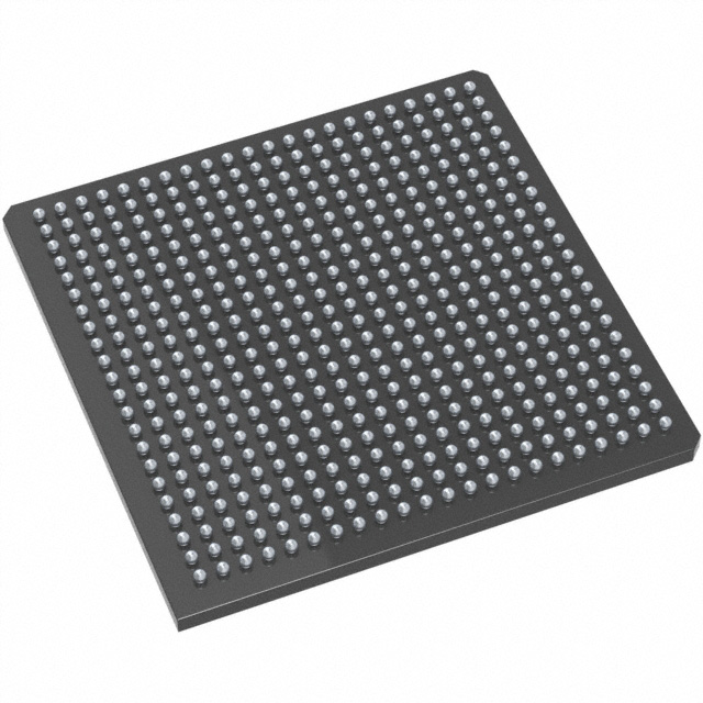
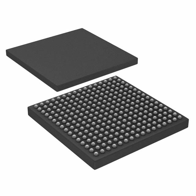
| Device Package | 256-FPBGA (17x17) | Grade | Commercial | Operating Temperature | 0°C – 70°C | ||
|---|---|---|---|---|---|---|---|
| Package / Case | 256-BGA | Number of I/O | 203 | Voltage | 2.25 V - 5.25 V | ||
| Mounting Method | Surface Mount | RoHS Compliance | RoHS non-compliant | REACH Compliance | REACH Unaffected | ||
| Moisture Sensitivity Level | 3 (168 Hours) | Number of LABs/CLBs | 6036 | Number of Logic Elements/Cells | 6036 | ||
| Number of Gates | 108000 | ECCN | 3A991D | HTS Code | 8542.39.0001 | ||
| Qualification | N/A |
Overview of A54SX72A-FFG256 – SX-A FPGA, 203 I/O, 256-BGA
The A54SX72A-FFG256 is a member of the SX-A family of nonvolatile FPGAs. It delivers a reconfigurable logic fabric with 6,036 logic elements and a device capacity of 108,000 system gates, targeting designs that require mid-range gate density and flexible I/O implementation.
Designed for mixed-voltage systems, this commercial-grade FPGA supports broad I/O flexibility and single-chip nonvolatile configuration, making it suitable for applications that need deterministic timing, configurable I/O standards, and on-board security features.
Key Features
- Core Performance — SX-A family performance characteristics include up to 250 MHz system performance and up to 350 MHz internal performance as documented for the family.
- Logic Capacity — Contains 6,036 logic elements (combinatorial cells and logic modules) and a device gate count of 108,000 system gates to implement medium-complexity designs.
- I/O Resources — 203 user-programmable I/O pins available for flexible interfacing; I/Os support hot-swap behavior and configurable weak pull-up or pull-down at power-up.
- Mixed-Voltage I/O Support — Configurable I/O support for 3.3 V / 5 V PCI, 5 V TTL, 3.3 V LVTTL, and 2.5 V LVCMOS2; devices support 2.5 V, 3.3 V, and 5 V mixed-voltage operation with 5 V input tolerance and 5 V drive strength.
- Nonvolatile, Single-Chip Configuration — Single-chip nonvolatile architecture removes the need for external configuration memory and simplifies system power-up sequencing.
- Security and Test — Includes Actel Secure Programming Technology (FuseLock™) to protect design IP and supports IEEE 1149.1 boundary-scan (JTAG) for board-level testability.
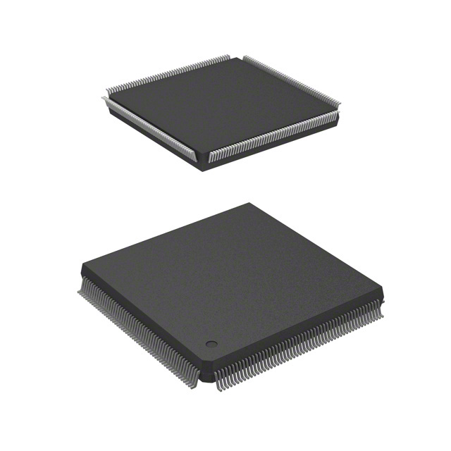
- Package and Thermal — Supplied in a 256-ball FBGA package (256-FPBGA, 17×17); commercial operating temperature range 0 °C to 70 °C.
- Power and Supply Range — Operates from 2.25 V to 5.25 V supply, allowing integration into a variety of legacy and modern power domains.
- Regulatory — RoHS-compliant device packaging.
Typical Applications
- Bus and Interface Bridging — PCI-compliant I/O options and hot-swap capable pins make the device suited for implementing bus bridges and interface logic where mixed-voltage signaling is required.
- Embedded Control and Glue Logic — Medium gate count and abundant I/O enable replacement of complex discrete logic and microcontroller glue logic in embedded control systems.
- Secure or IP-Sensitive Designs — Built-in secure programming (FuseLock™) supports applications that require protection of intellectual property or secure configuration storage.
- In-System Diagnostic and Verification — Family features for in-system diagnostics and verification support designs that need post-deployment validation and troubleshooting.
Unique Advantages
- Single-Chip Nonvolatile Solution: Eliminates external configuration components, reducing BOM complexity and simplifying board-level power sequencing.
- Broad I/O Flexibility: 203 user I/Os with support for multiple voltage standards and 5 V tolerance enable direct interfacing to a wide range of peripherals and legacy systems.
- Design Security Built In: FuseLock™ secure programming helps protect firmware and design IP from reverse engineering.
- Deterministic Timing: Family-level support for controlled, predictable timing behavior aids designs that require tight timing control and repeatability.
- Test and Debug Support: Boundary-scan (IEEE 1149.1) and in-system diagnostic capabilities reduce development and manufacturing test cycles.
- RoHS Compliance: Lead-free packaging supports regulatory and environmental requirements for deployment.
Why Choose A54SX72A-FFG256?
The A54SX72A-FFG256 delivers a balanced combination of logic capacity, flexible I/O, and single-chip nonvolatile configuration suited to mid-range FPGA applications. Its 6,036 logic elements and 108,000 system gates provide the resources needed for glue logic, interface bridging, and embedded control functions while keeping system-level integration compact.
With mixed-voltage I/O support, hot-swap capability, built-in security, and RoHS-compliant packaging, the device is intended for commercial designs that require reliable, testable, and secure programmable logic. It is a practical choice for engineers looking to reduce BOM count, simplify power sequencing, and protect design IP within a commercial temperature range.
Request a quote or submit an inquiry to receive pricing, lead-time, and available order quantities for the A54SX72A-FFG256. Our team can provide technical details and support to help determine fit for your design requirements.


Date Founded: 1989
Headquarters: Chandler, Arizona, USA
Employees: 22,000+
Revenue: $8.349 Billion
Certifications and Memberships: ISO9001:2015, IATF16949:2016, AS 9100D


