
AT40K10-2AQI
| Part Description |
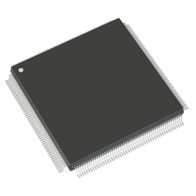
AT40K/KLV Field Programmable Gate Array (FPGA) IC 78 4608 576 100-TQFP |
|---|---|
| Quantity | 84 Available (as of October 8, 2026) |

| Product Category | Field Programmable Gate Array (FPGA) |
|---|---|
| Manufacturer | Microchip Technology |
| Manufacturing Status | Obsolete |
| Manufacturer Standard Lead Time | Contact Us |
| Datasheet |
Specifications & Environmental
| Device Package | 100-TQFP (14x14) | Grade | Industrial | Operating Temperature | -40°C – 85°C | ||
|---|---|---|---|---|---|---|---|
| Package / Case | 100-TQFP | Number of I/O | 78 | Voltage | 4.5 V - 5.5 V | ||
| Mounting Method | Surface Mount | RoHS Compliance | RoHS non-compliant | REACH Compliance | REACH Unaffected | ||
| Moisture Sensitivity Level | 3 (168 Hours) | Number of LABs/CLBs | 576 | Number of Logic Elements/Cells | 576 | ||
| Number of Gates | 20000 | ECCN | 3A991D | HTS Code | 8542.39.0001 | ||
| Qualification | N/A | Total RAM Bits | 4608 |
Overview of AT40K10-2AQI – AT40K/KLV FPGA, 78 I/O, 4,608-bit RAM, 576 Logic Elements, 100‑TQFP
The AT40K10-2AQI is an SRAM-based field programmable gate array (FPGA) designed for industrial applications. It combines 576 logic elements (cells) with approximately 4,608 bits of on-chip RAM and a usable gate count around 20,000 to implement computation-heavy and control functions.
Built for performance and reconfigurability, this device is suited for use as a DSP coprocessor, custom logic accelerator, or system control FPGA where deterministic timing, embedded memory, and reprogrammability are required.
Key Features
- Logic Capacity — 576 logic elements (cells) providing approximately 20,000 usable gates for mid-range complexity designs.
- Embedded Memory (FreeRAM) — Approximately 4,608 bits of distributed on-chip SRAM enabling flexible single- or dual-port memory constructs and scratchpad functions.
- Performance — Series-level characteristics include system speeds to 100 MHz, array multipliers >50 MHz and a 10 ns flexible SRAM cell time, supporting high-speed arithmetic and signal-processing tasks.
- I/O and Signal Drive — 78 I/O pins in the 100‑TQFP package with series-level programmable output drive and 3V/5V I/O capability noted in the family documentation; actual supply for this device is specified at 4.5 V to 5.5 V.
- Clocking — Series architecture provides up to 8 global clocks with low-skew distribution and configurable clock edges for timing flexibility.
- Package and Mounting — Supplied in a surface-mount 100‑TQFP (14 × 14 mm) package, suitable for standard PCB assembly processes.
- Industrial Temperature Range — Rated for operation from −40°C to 85°C and listed as Industrial grade for deployment in temperature-demanding environments.
- Standards and Compliance — RoHS compliant.
Typical Applications
- Signal Processing and DSP Acceleration — Implement FIR filters, FFTs, convolvers and other arithmetic-heavy operators using on-chip RAM and array multiplier resources.
- Video and Multimedia Processing — Offload compression/decompression tasks and vector multiply operations to the FPGA’s fast array multipliers and distributed SRAM.
- Custom I/O and Interface Logic — Handle protocol bridging, glue logic, and custom peripheral interfaces with the device’s programmable I/O and reconfigurable logic.
- Coprocessor and Embedded Acceleration — Augment microprocessor systems with application-specific accelerators for encryption, interpolation, or compute kernels.
Unique Advantages
- Balanced Mid‑range Capacity: 576 logic elements and ~20k gates enable complex control and signal-processing functions without excess cost or board area.
- Embedded Memory Flexibility: Approximately 4,608 bits of distributed SRAM allow creation of FIFOs, scratchpads, or coefficient storage without consuming logic resources.
- Reconfigurability: SRAM-based architecture supports in-system reprogramming and design iteration during development and deployment.
- Deterministic Timing Resources: Family-level support for up to 8 global clocks and fast SRAM access help achieve predictable timing for synchronous designs.
- Industrial Readiness: Surface-mount 100‑TQFP packaging, RoHS compliance, and an operating range of −40°C to 85°C make the device suitable for industrial applications.
Why Choose AT40K10-2AQI?
The AT40K10-2AQI positions itself as a practical, reprogrammable mid-range FPGA for designs that need embedded memory, deterministic clocking, and DSP-capable resources. With 576 logic elements, ~4.6k bits of on-chip RAM, and a supply range centered on 5 V operation, it provides a compact, industrial-grade option for accelerating computation, managing custom interfaces, and implementing adaptive logic.
Engineers seeking a field-updatable, performance-oriented FPGA with clear device-level specs (logic elements, RAM, I/O count, package, and temperature range) will find the AT40K10-2AQI well suited to prototypes and volume products where in-system reprogramming and on-chip memory are important.
Request a quote or submit a purchase inquiry to get pricing and lead-time information for the AT40K10-2AQI.






















Date Founded: 1989
Headquarters: Chandler, Arizona, USA
Employees: 22,000+
Revenue: $8.349 Billion
Certifications and Memberships: ISO9001:2015, IATF16949:2016, AS 9100D




