
AT40K20-2DQI
| Part Description |
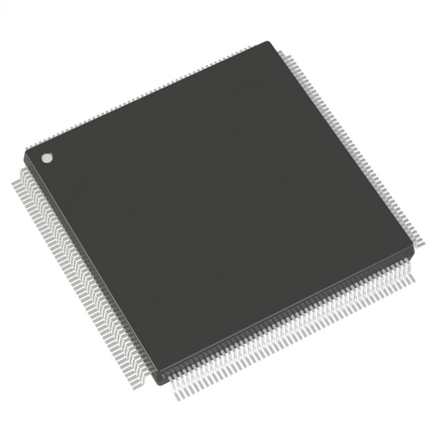
AT40K/KLV Field Programmable Gate Array (FPGA) IC 161 8192 1024 208-BFQFP |
|---|---|
| Quantity | 557 Available (as of October 8, 2026) |
| Product Category | Field Programmable Gate Array (FPGA) |
|---|---|
| Manufacturer | Microchip Technology |
| Manufacturing Status | Obsolete |
| Manufacturer Standard Lead Time | Contact Us |
| Datasheet |
Specifications & Environmental
| Device Package | 208-PQFP (28x28) | Grade | Industrial | Operating Temperature | -40°C – 85°C | ||
|---|---|---|---|---|---|---|---|
| Package / Case | 208-BFQFP | Number of I/O | 161 | Voltage | 4.5 V - 5.5 V | ||
| Mounting Method | Surface Mount | RoHS Compliance | RoHS non-compliant | REACH Compliance | REACH Unaffected | ||
| Moisture Sensitivity Level | 3 (168 Hours) | Number of LABs/CLBs | 1024 | Number of Logic Elements/Cells | 1024 | ||
| Number of Gates | 30000 | ECCN | 3A991D | HTS Code | 8542.39.0001 | ||
| Qualification | N/A | Total RAM Bits | 8192 |
Overview of AT40K20-2DQI – AT40K/KLV Field Programmable Gate Array (FPGA) IC 161 8192 1024 208-BFQFP
The AT40K20-2DQI is a 5V, surface-mount FPGA in a 208-BFQFP package built on the AT40K/AT40KLV series architecture. It provides 1,024 logic elements, approximately 8,192 bits of embedded RAM and 161 I/O pins, targeting industrial embedded and DSP-acceleration applications.
Designed for high-performance, reconfigurable system functions, this device combines distributed 10 ns SRAM, array multiplier support and multi-clock capabilities to accelerate computation-intensive tasks and simplify system integration.
Key Features
- Logic Fabric 1,024 logic elements (cells) delivering approximately 30,000 usable gates for implementing custom digital logic and control functions.
- Embedded Memory Approximately 8,192 bits of on-chip RAM with 10 ns SRAM performance and support for single- or dual-port, synchronous or asynchronous configurations at the series level.
- I/O and Drive 161 general-purpose I/O pins with 3V/5V capability at the series level and programmable output drive options described in the family datasheet.
- Clocking Multi-clock support from the AT40K series including up to 8 global clocks and additional dedicated PCI clocks for low-skew distribution and flexible timing control.
- DSP-Friendly Architecture Array multiplier support and direct cell-to-cell connectivity in the series facilitate fast arithmetic operations and vector multiplier implementations.
- Package & Mounting 208-BFQFP (208-PQFP 28×28) surface-mount package for compact PCB integration.
- Supply & Temperature 5V nominal supply range (4.5 V to 5.5 V) and industrial operating temperature range of −40°C to 85°C.
- Compliance & Environmental RoHS compliant.
Typical Applications
- DSP Acceleration Implement FIR filters, FFTs, convolvers and other computation-intensive blocks as a coprocessor to offload processors and improve throughput.
- Video & Multimedia Processing Support for fast array multipliers and embedded RAM enables coefficient storage and high-speed data paths used in video compression, decompression and image processing pipelines.
- Industrial Control Use the device’s logic elements, on-chip memory and robust operating range for motor control, sensor interfacing and real-time automation tasks.
- Custom I/O & Glue Logic Consolidate interface converters, bus bridging and protocol glue logic into a single FPGA to reduce board-level component count.
Unique Advantages
- On-Chip RAM Efficiency: Approximately 8,192 bits of embedded SRAM reduce external memory needs and simplify FIFO, scratchpad and buffer designs.
- Reconfigurable DSP Support: Series-level array multiplier architecture and direct cell interconnects accelerate arithmetic functions without heavy busing overhead.
- Multi-Clock Flexibility: Multiple global clocks and dedicated PCI clock options facilitate complex timing domains and low-skew distribution for synchronous designs.
- Industrial-Rated Operation: Specified for −40°C to 85°C operation and a 5V supply range, suitable for a wide range of industrial embedded environments.
- Compact Packaging: 208-BFQFP surface-mount package enables dense board layouts while providing a high pin count for flexible connectivity.
Why Choose AT40K20-2DQI?
The AT40K20-2DQI pairs a compact logic capacity with on-chip SRAM and series-proven FPGA architecture to deliver a practical platform for DSP acceleration, interface consolidation and industrial control. Its combination of 1,024 logic elements, approximately 8,192 bits of embedded memory and 161 I/Os makes it well suited for designs that need reconfigurable hardware with deterministic resource counts.
For teams developing industrial embedded systems or computation-heavy modules, this FPGA offers a balance of performance, reconfigurability and integration that supports iterative design updates and scalable implementations within the AT40K family ecosystem.
Request a quote or submit a pricing inquiry to check availability and secure parts for your next design.






















Date Founded: 1989
Headquarters: Chandler, Arizona, USA
Employees: 22,000+
Revenue: $8.349 Billion
Certifications and Memberships: ISO9001:2015, IATF16949:2016, AS 9100D




