
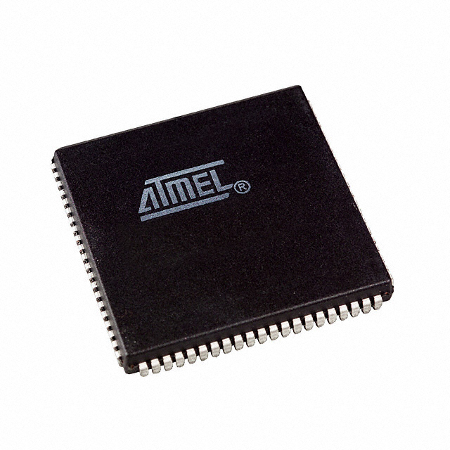
AT40K20-2BQI
| Part Description |
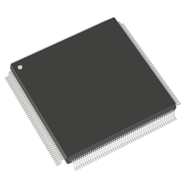
AT40K/KLV Field Programmable Gate Array (FPGA) IC 114 8192 1024 144-LQFP |
|---|---|
| Quantity | 1,260 Available (as of June 15, 2026) |

| Product Category | Field Programmable Gate Array (FPGA) |
|---|---|
| Manufacturer | Microchip Technology |
| Manufacturing Status | Obsolete |
| Manufacturer Standard Lead Time | Contact Us |
| Datasheet |
Specifications & Environmental
| Device Package | 144-LQFP (20x20) | Grade | Industrial | Operating Temperature | -40°C – 85°C | ||
|---|---|---|---|---|---|---|---|
| Package / Case | 144-LQFP | Number of I/O | 114 | Voltage | 4.5 V - 5.5 V | ||
| Mounting Method | Surface Mount | RoHS Compliance | RoHS non-compliant | REACH Compliance | REACH Unaffected | ||
| Moisture Sensitivity Level | 3 (168 Hours) | Number of LABs/CLBs | 1024 | Number of Logic Elements/Cells | 1024 | ||
| Number of Gates | 30000 | ECCN | 3A991D | HTS Code | 8542.39.0001 | ||
| Qualification | N/A | Total RAM Bits | 8192 |
Overview of AT40K20-2BQI – AT40K/KLV Field Programmable Gate Array (FPGA) IC, 114 I/O, 1,024 logic elements, 8,192 bits RAM, 144-LQFP
The AT40K20-2BQI is an SRAM-based field programmable gate array from Microchip Technology designed for mid-range gate-count applications. Built on the AT40K family architecture, it combines reconfigurable logic, distributed on-chip SRAM, and dedicated clocking to support computation-intensive tasks and adaptive designs.
This device targets applications such as DSP coprocessing, video and multimedia processing, and general-purpose embedded logic in industrial environments. Key value propositions include fast on-chip memory access, dynamic reconfigurability, and a robust industrial-grade temperature and supply specification for reliable deployment.
Key Features
- Core Performance — Ultra high-performance series architecture with documented system speeds to 100 MHz and array multipliers capable of >50 MHz; cells include internal tri-state capability for flexible routing and logic implementation.
- Logic Capacity — 1,024 logic elements (cells) supporting approximately 30,000 usable gates, suitable for mid-range integration of combinational and sequential logic.
- Embedded Memory (FreeRAM) — 8,192 bits of distributed, 10 ns programmable SRAM independent of logic cells, usable as single-port or dual-port, synchronous or asynchronous memory for FIFOs, scratch pads and temporary storage.
- I/O and Voltage — 114 general-purpose I/O pins and a 5 V-class supply range (4.5 V to 5.5 V), enabling use in 5 V systems while supporting flexible I/O drive options provided by the series architecture.
- Clocking — Dedicated global clock resources (8 global clocks available in the family) for low-skew distribution and configurable edge transitions to support timing-sensitive designs.
- Reconfigurability (Cache Logic) — Series-level support for dynamic full/partial in-system reconfiguration, enabling adaptive designs and rapid updates without losing stored data in specified modes.
- Package & Mounting — 144-LQFP (20×20) surface-mount package; industrial-grade construction and operating range.
- Environmental & Reliability — RoHS-compliant and specified for industrial operating temperatures from −40 °C to 85 °C.
Typical Applications
- DSP Coprocessing — Implement FIR filters, FFTs, convolvers and interpolators to offload computation from a host processor and accelerate signal-processing tasks.
- Video and Multimedia Processing — Use on-chip multipliers and distributed RAM to handle video compression, decompression and other media transforms that require fast, low-latency arithmetic.
- Data Buffers and FIFOs — Leverage the 8,192 bits of FreeRAM for temporary storage, buffering, and data-path staging in communication and streaming applications.
- Industrial Embedded Control — Deploy as configurable logic for motor control, sensor aggregation, and protocol bridging within the −40 °C to 85 °C operating range.
Unique Advantages
- Flexible on-chip memory: Distributed 10 ns SRAM (FreeRAM) provides single/dual-port, synchronous/asynchronous memory independent of logic cells, reducing external RAM needs and lowering BOM complexity.
- Reconfigurable design flow: Cache Logic dynamic reconfiguration enables partial or full in-system updates for adaptive algorithms and fast iteration during development and deployment.
- Deterministic clocking: Multiple global clocks deliver low-skew distribution and configurable edges, simplifying timing closure for high-speed designs.
- Industrial reliability: Surface-mount 144-LQFP packaging, industrial temperature rating (−40 °C to 85 °C) and RoHS compliance support long-term use in industrial applications.
- Balanced integration: Combination of ~30,000 gates, 1,024 logic elements and 114 I/Os provides a mid-range solution that balances logic density and I/O count for embedded systems.
- Design ecosystem compatibility: Series-level documentation highlights compatibility with industry-standard synthesis and simulation tools to streamline integration into existing toolchains.
Why Choose AT40K20-2BQI?
The AT40K20-2BQI offers a balanced FPGA solution for engineers who need mid-range gate density, fast on-chip memory, and industrial operating specifications. Its combination of 1,024 logic elements, approximately 8,192 bits of distributed SRAM, and dedicated clocking resources makes it well suited for DSP acceleration, streaming data handling, and adaptable embedded logic.
With a 5 V supply range, 114 I/Os, 144-LQFP surface-mount packaging, and RoHS-compliant industrial temperature rating, this device provides a reliable platform for production systems that require in-field configurability and efficient resource utilization.
Request a quote or submit a quote today to get pricing and availability for the AT40K20-2BQI and to discuss how it fits your next design.


Date Founded: 1989
Headquarters: Chandler, Arizona, USA
Employees: 22,000+
Revenue: $8.349 Billion
Certifications and Memberships: ISO9001:2015, IATF16949:2016, AS 9100D


