
AT40K20-2AJI
| Part Description |
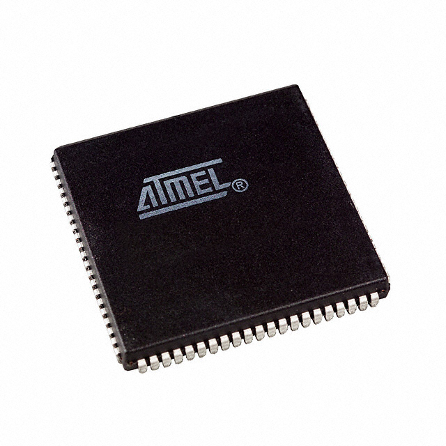
AT40K/KLV Field Programmable Gate Array (FPGA) IC 62 8192 1024 84-LCC (J-Lead) |
|---|---|
| Quantity | 472 Available (as of June 15, 2026) |
| Product Category | Field Programmable Gate Array (FPGA) |
|---|---|
| Manufacturer | Microchip Technology |
| Manufacturing Status | Obsolete |
| Manufacturer Standard Lead Time | Contact Us |
| Datasheet |
Specifications & Environmental
| Device Package | 84-PLCC (29.31x29.31) | Grade | Industrial | Operating Temperature | -40°C – 85°C | ||
|---|---|---|---|---|---|---|---|
| Package / Case | 84-LCC (J-Lead) | Number of I/O | 62 | Voltage | 4.5 V - 5.5 V | ||
| Mounting Method | Surface Mount | RoHS Compliance | RoHS non-compliant | REACH Compliance | REACH Unaffected | ||
| Moisture Sensitivity Level | 2 (1 Year) | Number of LABs/CLBs | 1024 | Number of Logic Elements/Cells | 1024 | ||
| Number of Gates | 30000 | ECCN | 3A991D | HTS Code | 8542.39.0001 | ||
| Qualification | N/A | Total RAM Bits | 8192 |
Overview of AT40K20-2AJI – SRAM-based FPGA, 62 I/O, 8,192-bit FreeRAM, 1,024 Logic Elements, 84‑PLCC
The AT40K20-2AJI is an SRAM-based Field Programmable Gate Array (FPGA) from Microchip Technology’s AT40K family. This device integrates approximately 1,024 logic elements with 8,192 bits of distributed on-chip RAM (FreeRAM) in an 84‑lead PLCC (J‑lead) package, targeting medium-density programmable logic needs.
Designed for embedded and industrial applications, the AT40K20-2AJI supports high-speed arithmetic and control functions — suitable for DSP coprocessor roles, data processing, and other tasks that benefit from on-chip RAM and reconfigurable logic in a 5 V supply environment.
Key Features
- Logic Capacity Approximately 1,024 logic elements (cells) enabling medium-density logic implementations and custom combinational/sequential functions.
- Embedded Memory (FreeRAM) 8,192 bits of distributed, flexible on-chip SRAM; supports single/dual-port and synchronous/asynchronous operation with 10 ns class access time per the series specification.
- Performance Series-level capabilities include system speeds to 100 MHz and array multiplier performance >50 MHz, enabling accelerated arithmetic operations (series data).
- I/O and Drive 62 user I/O pins for external interfacing and peripheral connectivity in the PLCC package.
- Clocking Series features include multiple global clocks and programmable clock control which support low-skew distribution and flexible timing management.
- Supply and Mounting Operates from 4.5 V to 5.5 V and is available in a surface-mount 84‑PLCC (29.31 × 29.31 mm) package with J‑lead (84‑LCC) terminations.
- Industrial Temperature Range Rated for operation from −40 °C to 85 °C, suited for industrial environments.
- Standards & Compliance RoHS compliant.
Typical Applications
- DSP Coprocessors Implement arithmetic-intensive blocks such as FIR filters and FFTs using on-chip multipliers and FreeRAM for coefficient and data storage.
- Video and Multimedia Processing Accelerate vector and array operations for codecs, compression/decompression, and other media pipelines leveraging the device’s array multiplier and embedded SRAM.
- Encryption and Signal Processing Custom cryptographic engines and convolutional transforms can be mapped to the FPGA’s logic and distributed RAM for low-latency processing.
- Industrial Control Control logic, sensor interfacing, and protocol handling in industrial systems using the device’s I/O, temperature range, and 5 V supply compatibility.
Unique Advantages
- Flexible On-Chip Memory: The AT40K20-2AJI’s 8,192 bits of distributed FreeRAM enable efficient buffer, FIFO, and coefficient storage without consuming logic elements.
- Medium-Density Programmability: Approximately 1,024 logic elements provide a compact, reprogrammable platform for consolidating glue logic, control functions, and moderate DSP tasks on a single device.
- 5 V System Compatibility: With a 4.5–5.5 V supply range, the device integrates into legacy 5 V systems while supporting industrial deployment across −40 °C to 85 °C.
- Package and Mounting Flexibility: Available in an 84‑lead PLCC (J‑lead) surface-mount package (29.31 × 29.31 mm) for board-level designs that require PLCC form factor.
- Series-Level Performance Features: Series capabilities such as 10 ns SRAM access, array multipliers, and multi-clock support enable higher-throughput designs when leveraged by appropriate tool flows and design practices.
- RoHS Compliant: Meets RoHS requirements for lead-free manufacturing processes.
Why Choose AT40K20-2AJI?
The AT40K20-2AJI positions itself as a reliable medium-density SRAM-based FPGA for industrial and embedded designs that require on-chip memory, reprogrammability, and 5 V operation. Its combination of approximately 1,024 logic elements, 8,192 bits of distributed FreeRAM, and series-level performance features makes it suitable for offloading DSP tasks, accelerating data-path operations, and consolidating control logic in compact PLCC packages.
Engineers seeking a reconfigurable device with industrial temperature capability and PLCC mounting can leverage the AT40K20-2AJI to simplify BOM and enable adaptable, field-updatable functionality while maintaining compatibility with 5 V system environments.
Request a quote or submit an inquiry to obtain pricing and availability for the AT40K20-2AJI. Provide your quantity and delivery requirements to receive a tailored response.


Date Founded: 1989
Headquarters: Chandler, Arizona, USA
Employees: 22,000+
Revenue: $8.349 Billion
Certifications and Memberships: ISO9001:2015, IATF16949:2016, AS 9100D


