
AT40K20-2EQI
| Part Description |
AT40K/KLV Field Programmable Gate Array (FPGA) IC 193 8192 1024 240-BFQFP |
|---|---|
| Quantity | 887 Available (as of October 7, 2026) |

| Product Category | Field Programmable Gate Array (FPGA) |
|---|---|
| Manufacturer | Microchip Technology |
| Manufacturing Status | Obsolete |
| Manufacturer Standard Lead Time | Contact Us |
| Datasheet |
Specifications & Environmental
| Device Package | 240-PQFP (32x32) | Grade | Industrial | Operating Temperature | -40°C – 85°C | ||
|---|---|---|---|---|---|---|---|
| Package / Case | 240-BFQFP | Number of I/O | 193 | Voltage | 4.5 V - 5.5 V | ||
| Mounting Method | Surface Mount | RoHS Compliance | RoHS non-compliant | REACH Compliance | REACH Unaffected | ||
| Moisture Sensitivity Level | 3 (168 Hours) | Number of LABs/CLBs | 1024 | Number of Logic Elements/Cells | 1024 | ||
| Number of Gates | 30000 | ECCN | 3A991D | HTS Code | 8542.39.0001 | ||
| Qualification | N/A | Total RAM Bits | 8192 |
Overview of AT40K20-2EQI – FPGA, 1,024 logic elements, 8,192-bit RAM, 240-BFQFP
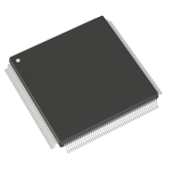
The AT40K20-2EQI is an SRAM-based Field Programmable Gate Array (FPGA) in a 240-pin BFQFP package designed for high-performance, reconfigurable logic. It provides 1,024 logic elements, approximately 8,192 bits of embedded RAM, and 193 I/O pins to support complex digital designs.
Built on the AT40K family architecture, the device targets applications that need fast on-chip memory access, multiple global clocks and in-system reconfigurability. Its combination of 10 ns distributed SRAM, global clock resources and industrial-grade operating range make it suitable for demanding embedded and DSP-oriented designs.
Key Features
- Logic Capacity — 1,024 logic elements (cells) and approximately 30,000 usable gates provide programmable logic resources for mid-range designs.
- Embedded Memory (FreeRAM) — Distributed 10 ns SRAM totaling 8,192 bits that can be implemented as single- or dual-port, synchronous or asynchronous RAM without consuming separate logic resources.
- I/O and Interface — 193 I/O pins with family-level PCI-compliant I/O architecture and 3V/5V capability; programmable output drive and fast, flexible array access for pin locking.
- Clocking — Up to 8 global clocks with low-skew distribution, programmable edge transitions, and distributed clock shutdown for power management.
- Reconfigurability — Cache Logic dynamic partial/full in-system reconfigurability with unlimited re-programmability via serial or parallel modes for adaptive designs and runtime updates.
- Performance — Family features include system speeds to 100 MHz, array multipliers >50 MHz, and 10 ns SRAM timing for high-throughput implementations.
- Package & Supply — 240-BFQFP (supplier package: 240-PQFP, 32×32) with a recommended supply range of 4.5 V to 5.5 V.
- Industrial Temperature Range — Rated for operation from –40°C to 85°C; RoHS compliant.
Typical Applications
- DSP Coprocessing — Implement FIR filters, FFTs, convolvers and other compute-intensive blocks that benefit from fast array multipliers and distributed RAM.
- Video and Multimedia — Use reconfigurable logic and on-chip memory for video compression/decompression, transforms and real-time data paths.
- PCI/High-speed I/O Systems — Leverage the PCI-compliant I/O architecture and programmable drive strengths for board-level interface logic and protocol glue.
- Adaptive In-System Logic — Employ Cache Logic partial/full reconfiguration to update algorithms or coefficients in-system without data loss.
Unique Advantages
- Distributed Fast SRAM — On-chip 10 ns FreeRAM enables low-latency data storage and scratchpad memory without consuming logic elements, simplifying FIFOs and buffers.
- Dynamic Reconfiguration — Cache Logic supports full or partial reconfiguration in-system, enabling field updates and adaptive algorithm changes.
- Robust Clocking — Eight global clocks with programmable transitions and low skew enable multi-clock domain designs and precise timing control.
- I/O Flexibility — High pin count (193) with 3V/5V capability and programmable output drive supports mixed-voltage board designs and a wide range of peripherals.
- Production-Ready Package — 240-pin BFQFP (240-PQFP footprint) provides an industry-standard surface-mount form factor for production deployment.
- Design Ecosystem Integration — Family-level support for industry-standard design flows and automatic component generators accelerates development and reuse of IP.
Why Choose AT40K20-2EQI?
The AT40K20-2EQI combines mid-range logic capacity with high-performance embedded SRAM and flexible clocking to address DSP, multimedia and interface-intensive designs. Its industrial temperature rating, RoHS compliance and industry-standard package make it suitable for production embedded systems requiring reconfigurability and robust operation.
Developers benefit from the family’s reconfiguration features and ecosystem support to iterate quickly and scale solutions across larger AT40K devices when needed, providing long-term design flexibility and reduced time-to-market.
Request a quote or submit an inquiry to check pricing and availability for the AT40K20-2EQI and to discuss how it fits your next design.

























Date Founded: 1989
Headquarters: Chandler, Arizona, USA
Employees: 22,000+
Revenue: $8.349 Billion
Certifications and Memberships: ISO9001:2015, IATF16949:2016, AS 9100D




