
AT40K20AL-1AJC
| Part Description |
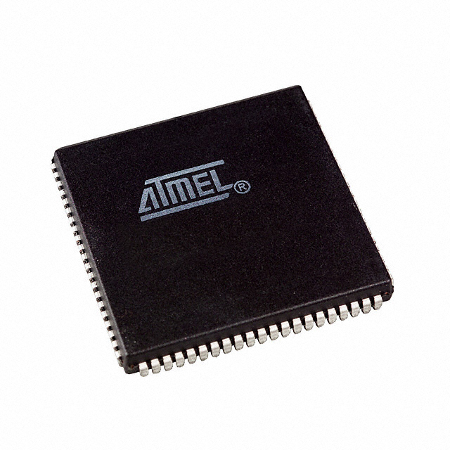
AT40KAL Field Programmable Gate Array (FPGA) IC 62 8192 1024 84-LCC (J-Lead) |
|---|---|
| Quantity | 668 Available (as of October 8, 2026) |
| Product Category | Field Programmable Gate Array (FPGA) |
|---|---|
| Manufacturer | Microchip Technology |
| Manufacturing Status | Obsolete |
| Manufacturer Standard Lead Time | Contact Us |
| Datasheet |
Specifications & Environmental
| Device Package | 84-PLCC (29.31x29.31) | Grade | Commercial | Operating Temperature | 0°C – 70°C | ||
|---|---|---|---|---|---|---|---|
| Package / Case | 84-LCC (J-Lead) | Number of I/O | 62 | Voltage | 3 V - 3.6 V | ||
| Mounting Method | Surface Mount | RoHS Compliance | RoHS non-compliant | REACH Compliance | REACH Unaffected | ||
| Moisture Sensitivity Level | 2 (1 Year) | Number of LABs/CLBs | 1024 | Number of Logic Elements/Cells | 1024 | ||
| Number of Gates | 30000 | ECCN | 3A991D | HTS Code | 8542.39.0001 | ||
| Qualification | N/A | Total RAM Bits | 8192 |
Overview of AT40K20AL-1AJC – AT40KAL FPGA, 1,024 logic elements, 8,192-bit RAM, 84-LCC (J-Lead)
The AT40K20AL-1AJC is an SRAM-based Field Programmable Gate Array (FPGA) from the AT40KAL family provided by Microchip Technology. It delivers reprogrammable logic with 1,024 logic elements, 8,192 bits of embedded RAM and approximately 30,000 logic-equivalent gates in an 84-pin LCC (J-Lead) package.
Designed for mid-range, reconfigurable designs, this device targets applications that benefit from fast on-chip RAM, dynamic partial/full reconfiguration and flexible clocking options as described for the AT40KAL series.
Key Features
- Core Architecture SRAM-based FPGA family features including Cache Logic dynamic reconfiguration capabilities as described in the AT40KAL series documentation.
- Logic Density 1,024 logic elements (cells) providing approximately 30,000 gates for medium-complexity designs.
- Embedded Memory (FreeRAM) 8,192 total RAM bits of distributed 10 ns SRAM enabling multiple small independent single- or dual-port RAM functions without consuming additional logic resources.
- I/O 62 I/O pins supporting flexible interfacing in the 84-LCC (J-Lead) package.
- Clocking Series-level capability includes multiple global clocks and low-skew distribution as part of the AT40KAL architecture.
- Power Operates from a 3.0 V to 3.6 V supply.
- Package & Mounting 84-LCC (J-Lead) package; supplier device package listed as 84-PLCC with 29.31 × 29.31 mm footprint; surface-mount mounting type.
- Commercial Temperature Grade Rated for 0 °C to 70 °C operation.
- Standards & Compliance RoHS compliant.
- Design Ecosystem AT40KAL series documentation highlights support for industry-standard synthesis and design tools and migration paths for production scaling.
Typical Applications
- DSP and Coprocessing Implement arithmetic-intensive functions such as FIR filters, FFTs and array multipliers using the device’s distributed SRAM and logic resources.
- Video and Multimedia Suitable for building blocks used in video compression, decompression and other multimedia signal processing workflows.
- Encryption and Security Hardware-accelerated cryptographic and data-processing functions can leverage the on-chip RAM and reconfigurable logic.
- Interface and Glue Logic Mid-density I/O and reprogrammability make the device useful for protocol bridging, pin reassignment and custom peripheral interfacing.
Unique Advantages
- Flexible Embedded RAM: 8,192 bits of distributed 10 ns SRAM enable efficient FIFO, scratchpad and dual/single-port RAM designs without sacrificing logic elements.
- Dynamic Reconfiguration (Cache Logic): Series-level partial or full in-system reconfiguration allows adaptive updates and design changes without losing stored data.
- Mid-Range Gate Count: Roughly 30,000 gates and 1,024 logic elements address medium-complexity designs that require a balance of density and cost.
- Compact Package Options: 84-LCC (J-Lead) surface-mount package fits designs where a small footprint and standard PLCC-style pinout are required.
- Design Tool Integration: The AT40KAL family is documented to integrate with industry-standard synthesis and simulation tools, facilitating development and migration to production.
- RoHS Compliance: Meets RoHS environmental requirements for lead-free manufacturing flows.
Why Choose AT40K20AL-1AJC?
The AT40K20AL-1AJC is positioned for engineers needing a reprogrammable, SRAM-based FPGA with medium logic density and on-chip RAM optimized for DSP-style tasks and adaptive designs. Its combination of approximately 1,024 logic elements, 8,192 bits of distributed RAM and series-level reconfiguration capability provides a practical balance of performance and flexibility for embedded signal processing, interface logic and hardware acceleration.
With a 3.0–3.6 V supply range, surface-mount 84-LCC packaging and commercial-grade temperature rating, this device suits a wide range of standard commercial applications where RoHS compliance and integration with common design toolchains are important.
Request a quote or submit a purchase inquiry for the AT40K20AL-1AJC to receive pricing and availability details.























Date Founded: 1989
Headquarters: Chandler, Arizona, USA
Employees: 22,000+
Revenue: $8.349 Billion
Certifications and Memberships: ISO9001:2015, IATF16949:2016, AS 9100D




