
AT6010A-4AC
| Part Description |
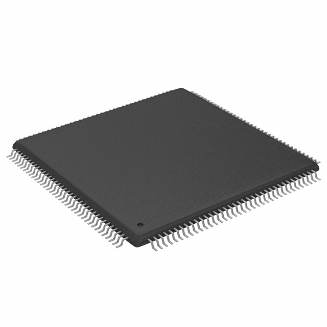
AT6000(LV) Field Programmable Gate Array (FPGA) IC 120 6400 144-LQFP |
|---|---|
| Quantity | 297 Available (as of June 14, 2026) |

| Product Category | Field Programmable Gate Array (FPGA) |
|---|---|
| Manufacturer | Microchip Technology |
| Manufacturing Status | Obsolete |
| Manufacturer Standard Lead Time | Contact Us |
| Datasheet |
Specifications & Environmental
| Device Package | 144-LQFP (20x20) | Grade | Commercial | Operating Temperature | 0°C – 70°C | ||
|---|---|---|---|---|---|---|---|
| Package / Case | 144-LQFP | Number of I/O | 120 | Voltage | 4.75 V - 5.25 V | ||
| Mounting Method | Surface Mount | RoHS Compliance | RoHS non-compliant | REACH Compliance | REACH Unaffected | ||
| Moisture Sensitivity Level | 3 (168 Hours) | Number of LABs/CLBs | N/A | Number of Logic Elements/Cells | 6400 | ||
| Number of Gates | 30000 | ECCN | 3A991D | HTS Code | 8542.39.0001 | ||
| Qualification | N/A |
Overview of AT6010A-4AC – AT6000(LV) Field Programmable Gate Array (FPGA) IC 120 6400 144-LQFP
The AT6010A-4AC is an SRAM-based Field Programmable Gate Array from the AT6000(LV) family. It implements a symmetrical array of 6,400 cells and is designed for reconfigurable coprocessors and compute‑intensive logic where adaptive hardware and hardware acceleration are required.
Built for high-speed designs, this device supports system speeds greater than 100 MHz and provides a flexible, programmable I/O fabric in a 144‑LQFP (20 × 20) surface-mount package. It is supplied for commercial grade applications with a 0 °C to 70 °C operating range and RoHS compliance.
Key Features
- Core architecture — Symmetrical array of 6,400 cells delivering up to 30,000 usable gates and up to 6,400 registers for dense, compute‑oriented logic implementations.
- Performance — System speeds >100 MHz and flip-flop toggle rates >250 MHz; measured input and output delays are documented for tight timing control (1.2 ns/1.5 ns input delay, 3.0 ns/6.0 ns output delay).
- I/O and interfacing — 120 user I/Os (part-specific) with programmable I/O options: TTL/CMOS input thresholds, open-collector/tristate outputs, programmable slew-rate control, and 16 mA drive (combinable to 64 mA).
- In-system reconfiguration — Supports complete and partial in-system reconfiguration with no loss of data or machine state, enabling adaptive hardware updates and runtime flexibility.
- Power — Low-power operation with standby currents as low as specified for the series and typical operating current ranges published for design planning; supports 5.0 V operation with a supply range of 4.75 V to 5.25 V.
- Clocking — Independently controlled column clocks and resets with clock skew less than 1 ns across the chip, enabling deterministic timing for column-structured logic.
- Package and mounting — 144‑LQFP (20 × 20) supplier package; surface-mount mounting for standard PCB assembly processes.
- Process and testing — Devices manufactured on a single‑poly, double‑metal CMOS process and 100% factory tested as documented for the series.
Typical Applications
- Reconfigurable coprocessors — Implement custom acceleration functions and offload compute‑intensive tasks using the device’s dense logic and in-system reconfiguration.
- Hardware acceleration — Deploy adaptive hardware blocks and cache-logic style accelerators to speed critical data paths in digital systems.
- High-speed digital processing — Use the device’s >100 MHz system speeds and low clock skew for timing-sensitive, high-throughput logic functions.
- Custom I/O interfaces — Leverage programmable I/O thresholds, slew-rate control and combinable drive strength for bespoke peripheral or bus interfacing needs.
Unique Advantages
- Flexible in-system reconfiguration: Complete and partial reconfiguration capability enables field updates and runtime adaptation without losing data or machine state.
- High logic density: 6,400 cells and up to 30,000 usable gates provide capacity for complex, compute-focused designs within a single FPGA package.
- Programmable, high-drive I/O: TTL/CMOS thresholds, open-collector/tristate outputs, programmable slew-rate, and up to 16 mA per pin (combinable to 64 mA) simplify heterogeneous interface design.
- Deterministic clocking: Independently controlled column clocks/resets and sub‑nanosecond skew across the chip support predictable timing across large arrays of logic.
- Commercial readiness and compliance: Surface-mount 144‑LQFP package, commercial operating range (0 °C to 70 °C), and RoHS compliance support mainstream electronic product development.
- Proven manufacturing and tool support: 0.6 µm CMOS process and 100% factory testing, combined with supported development tools for design entry and implementation.
Why Choose AT6010A-4AC?
The AT6010A-4AC combines substantial logic capacity, flexible I/O and deterministic clocking to address compute-intensive and reconfigurable tasks in commercial electronic systems. Its in-system reconfiguration and programmable interfaces make it suitable for designs that require field updates, adaptive hardware, or custom peripheral connectivity.
This device is aimed at designers who need a reliable, high-speed FPGA with clear electrical and mechanical characteristics—such as a 4.75 V to 5.25 V supply range, 0 °C to 70 °C operating window, and a 144‑LQFP surface-mount package—backed by factory testing and documented series-level performance.
Request a quote or submit a purchase inquiry to get lead-time and pricing information for the AT6010A-4AC. Our team can provide availability details and help with ordering quantities to match your project timeline.


Date Founded: 1989
Headquarters: Chandler, Arizona, USA
Employees: 22,000+
Revenue: $8.349 Billion
Certifications and Memberships: ISO9001:2015, IATF16949:2016, AS 9100D


