
AT6010A-2AC
| Part Description |
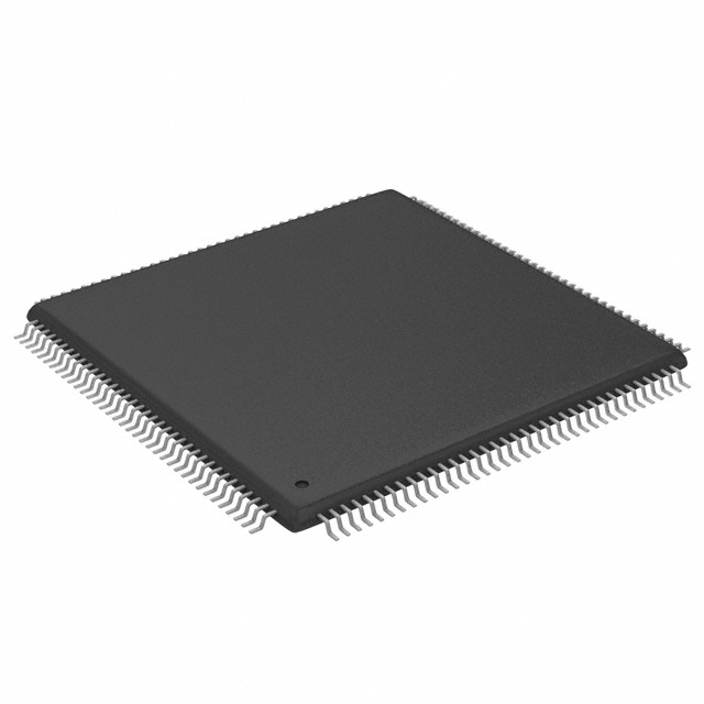
AT6000(LV) Field Programmable Gate Array (FPGA) IC 120 6400 144-LQFP |
|---|---|
| Quantity | 613 Available (as of June 10, 2026) |

| Product Category | Field Programmable Gate Array (FPGA) |
|---|---|
| Manufacturer | Microchip Technology |
| Manufacturing Status | Obsolete |
| Manufacturer Standard Lead Time | Contact Us |
| Datasheet |
Specifications & Environmental
| Device Package | 144-LQFP (20x20) | Grade | Commercial | Operating Temperature | 0°C – 70°C | ||
|---|---|---|---|---|---|---|---|
| Package / Case | 144-LQFP | Number of I/O | 120 | Voltage | 4.75 V - 5.25 V | ||
| Mounting Method | Surface Mount | RoHS Compliance | RoHS non-compliant | REACH Compliance | REACH Unaffected | ||
| Moisture Sensitivity Level | 3 (168 Hours) | Number of LABs/CLBs | N/A | Number of Logic Elements/Cells | 6400 | ||
| Number of Gates | 30000 | ECCN | 3A991D | HTS Code | 8542.39.0001 | ||
| Qualification | N/A |
Overview of AT6010A-2AC – AT6000(LV) Field Programmable Gate Array (FPGA) IC, 120 I/O, 6,400 Logic Elements, 144-LQFP
The AT6010A-2AC is an SRAM-based Field Programmable Gate Array (FPGA) designed for reconfigurable, compute‑intensive logic. Built on the AT6000(LV) architecture, it delivers a symmetrical cell array and a flexible busing network to implement adaptive hardware and hardware acceleration.
With 6,400 logic elements (cells), approximately 30,000 usable gates and 120 user I/O in a 144‑LQFP (20×20) package, the device targets high-speed system designs that require programmable I/O and column-based clock/reset control while operating within commercial temperature and voltage ranges.
Key Features
- Core Logic 6,400 logic elements (cells) and up to 30,000 usable gates provide dense, reconfigurable logic resources suitable for compute‑intensive functions.
- Performance System speeds greater than 100 MHz with flip‑flop toggle rates above 250 MHz; input delays around 1.2 ns / 1.5 ns and output delays around 3.0 ns / 6.0 ns as documented for the series.
- I/O and Interfaces 120 user I/O with independently configurable I/O supporting TTL/CMOS input thresholds, open‑collector/tristate outputs, programmable slew‑rate control and I/O drive of 16 mA (combinable to 64 mA).
- Clocking and Reset Independently controlled column clocks and column resets with clock skew of less than 1 ns across the chip enable tight timing coordination for multi‑clock designs.
- Power Low‑power characteristics for the series, with standby currents as low as 500 μA / 200 μA and typical operating currents reported across devices from 15 mA up to 170 mA.
- Package & Mounting 144‑lead LQFP (20×20) surface‑mount package for compact board integration and standard assembly processes.
- Voltage & Temperature Supports standard voltage operation (5.0 V, VCC = 4.75 V to 5.25 V) and low‑voltage operation options shown in the series documentation; commercial grade operation from 0 °C to 70 °C.
- Compliance RoHS compliant.
Typical Applications
- Reconfigurable Coprocessors Offload compute‑intensive algorithms and accelerate processing tasks by implementing custom logic kernels in the FPGA fabric.
- Hardware Acceleration Implement Cache Logic and adaptive hardware to speed critical data paths and reduce latency in signal and data processing systems.
- Interface Bridging & Glue Logic Use the device’s configurable I/O and programmable drive/slew features to implement interface conversion and complex glue logic between subsystems.
- Prototyping and Algorithm Development Rapidly iterate hardware designs leveraging in‑system reconfiguration for testing alternate architectures without board redesign.
Unique Advantages
- Substantial Logic Density: 6,400 logic elements and ~30,000 gates enable implementation of sizable custom datapaths and control logic within a single device, reducing board-level component count.
- Flexible, High‑Speed Clocking: Independently controlled column clocks/resets and <1 ns clock skew across the chip simplify timing closure for multi‑clock designs.
- Programmable, Robust I/O: TTL/CMOS thresholds, open‑collector/tristate options, programmable slew and up to 16 mA per I/O (combinable) support a wide range of external interface requirements.
- Low Power Operation: Series‑documented low standby currents and modest operating current ranges help minimize system power in both idle and active states.
- Board‑Level Convenience: Standard 144‑LQFP (20×20) surface‑mount package eases placement in space‑constrained mid‑range designs and supports common assembly flows.
- Commercial Temperature Range: Specified for 0 °C to 70 °C operation to match common commercial and enterprise applications.
Why Choose AT6010A-2AC?
The AT6010A-2AC combines a high count of logic elements with flexible clocking and programmable I/O, making it well suited for reconfigurable coprocessor roles, hardware acceleration and complex glue logic in commercial systems. Its 144‑LQFP package and surface‑mount form factor support compact board layouts while maintaining accessible I/O.
For designers seeking a commercially graded FPGA with documented performance characteristics from the AT6000(LV) series—such as >100 MHz system speeds, configurable I/O standards, and low standby currents—the AT6010A-2AC offers a balanced platform for developing high‑speed, adaptive hardware solutions.
Request a quote or submit an inquiry to receive pricing and availability information for the AT6010A-2AC.


Date Founded: 1989
Headquarters: Chandler, Arizona, USA
Employees: 22,000+
Revenue: $8.349 Billion
Certifications and Memberships: ISO9001:2015, IATF16949:2016, AS 9100D


