
AT6010-2QI
| Part Description |
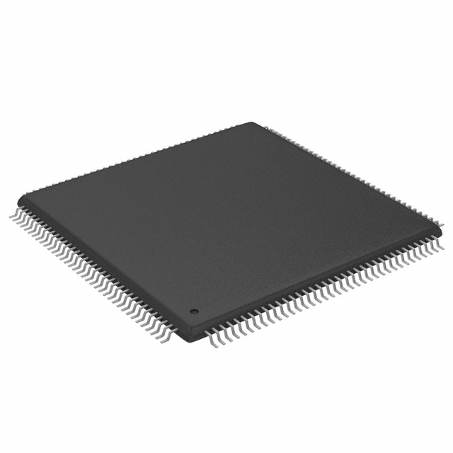
AT6000(LV) Field Programmable Gate Array (FPGA) IC 108 6400 132-BQFP Bumpered |
|---|---|
| Quantity | 347 Available (as of June 10, 2026) |

| Product Category | Field Programmable Gate Array (FPGA) |
|---|---|
| Manufacturer | Microchip Technology |
| Manufacturing Status | Obsolete |
| Manufacturer Standard Lead Time | Contact Us |
| Datasheet |
Specifications & Environmental
| Device Package | 132-BQFP (27.44x27.44) | Grade | Industrial | Operating Temperature | -40°C – 85°C | ||
|---|---|---|---|---|---|---|---|
| Package / Case | 132-BQFP Bumpered | Number of I/O | 108 | Voltage | 4.5 V - 5.5 V | ||
| Mounting Method | Surface Mount | RoHS Compliance | RoHS non-compliant | REACH Compliance | REACH Unaffected | ||
| Moisture Sensitivity Level | 3 (168 Hours) | Number of LABs/CLBs | N/A | Number of Logic Elements/Cells | 6400 | ||
| Number of Gates | 30000 | ECCN | 3A991D | HTS Code | 8542.39.0001 | ||
| Qualification | N/A |
Overview of AT6010-2QI – AT6000(LV) FPGA, 132‑BQFP (108 I/O, 6,400 logic elements)
The AT6010-2QI is an SRAM-based Field Programmable Gate Array (FPGA) from the AT6000(LV) family designed for reconfigurable, compute‑intensive logic. It delivers a symmetrical cell array architecture with 6,400 logic elements and a 132‑pin bumpered BQFP surface‑mount package for space‑efficient board integration.
Targeted at industrial applications, the device supports in‑system reconfiguration and programmable I/O, providing designers with high-performance, adaptable hardware for coprocessing, protocol bridging and custom logic acceleration while operating across a 4.5 V to 5.5 V supply and a –40 °C to 85 °C temperature range.
Key Features
- Core Architecture — 6,400 logic elements (cells) arranged in a symmetrical grid and a flexible busing network to support efficient routing and dense logic implementation.
- Logic Capacity — Approximately 30,000 gates and up to 6,400 registers for implementing compute‑intensive functions and cache logic‑style acceleration.
- I/O Flexibility — 108 user I/Os with independently configurable input thresholds (TTL/CMOS), open‑collector/tristate options, programmable slew‑rate control and 16 mA drive per pin (combinable to higher drive).
- Performance Characteristics — Series-level performance indicators include system speeds greater than 100 MHz and flip‑flop toggle rates above 250 MHz, with sub‑nanosecond clock skew control across the array.
- In‑System Reconfiguration — Supports complete and partial in‑system reconfiguration without loss of data or machine state, enabling adaptive hardware updates and iterative refinement in the field.
- Power — Operates from a 4.5 V to 5.5 V supply. Series data indicates very low standby current (on the order of hundreds of microamps) and typical operating currents in the tens to low hundreds of milliamps, enabling low‑power system options.
- Package & Mounting — 132‑pin BQFP (bumpered) package, 27.44 mm × 27.44 mm, surface‑mount mounting for streamlined PCB assembly.
- Industrial Temperature Range & Compliance — Rated for –40 °C to 85 °C operation and RoHS compliant for industrial deployments.
- Clocking and Control — Independently controlled column clocks and resets with tight skew control to support synchronous, high‑speed implementations.
- On‑chip Memory — No embedded RAM bits specified (Total RAM Bits: 0), allowing designers to pair the device with external memory architectures as required.
Typical Applications
- Compute Acceleration — Implement hardware acceleration and cache‑logic style functions for offloading compute‑intensive tasks from a host processor.
- Reconfigurable Coprocessors — Use complete or partial in‑system reconfiguration to adapt coprocessor functionality on demand without losing machine state.
- Interface Bridging & Protocol Conversion — Leverage 108 programmable I/Os and flexible drive/threshold options to build custom interface bridges and protocol translators.
- Industrial Control — Deploy in industrial control and automation systems that require industrial temperature ratings, deterministic timing and robust I/O configurability.
- Prototyping & Design Migration — Consistent pin locations within the AT6000 series simplify migration and iterative prototyping across family members.
Unique Advantages
- Reconfigurable without State Loss — Complete and partial in‑system reconfiguration enables field updates and adaptive hardware behavior while preserving data and machine state.
- Deterministic, High‑Speed Operation — Series performance metrics such as >100 MHz system speeds and <1 ns clock skew provide deterministic timing for high‑speed logic paths.
- Flexible, Programmable I/O — Independently configurable I/O with programmable thresholds, slew rate and combinable drive reduce the need for external level‑shifters and drivers.
- Industrial Reliability — –40 °C to 85 °C operating range and RoHS compliance make the device suitable for demanding industrial environments.
- Compact Surface‑Mount Package — 132‑pin bumpered BQFP package provides a balance of I/O count and board footprint for compact system designs.
- Proven Development Flow — Supported by the AT6000 series development tools for PC and workstation design entry and programming, accelerating time to prototype.
Why Choose AT6010-2QI?
The AT6010-2QI combines a 6,400‑cell SRAM FPGA fabric with 108 programmable I/Os and a compact 132‑pin BQFP package, making it well suited for industrial designers who need reconfigurable, high‑performance logic in a surface‑mount form factor. Its in‑system reconfiguration capability and flexible clocking model enable adaptive hardware acceleration and deterministic timing for compute‑intensive tasks.
This device is positioned for customers building reconfigurable coprocessors, protocol bridges and industrial control logic who require predictable performance, configurable I/O and industrial temperature operation. Support from the AT6000 series development environment helps streamline design entry and iteration across the family.
Request a quote or submit an inquiry to receive pricing and availability for the AT6010-2QI and to discuss how it can fit your next FPGA‑based design.


Date Founded: 1989
Headquarters: Chandler, Arizona, USA
Employees: 22,000+
Revenue: $8.349 Billion
Certifications and Memberships: ISO9001:2015, IATF16949:2016, AS 9100D


