
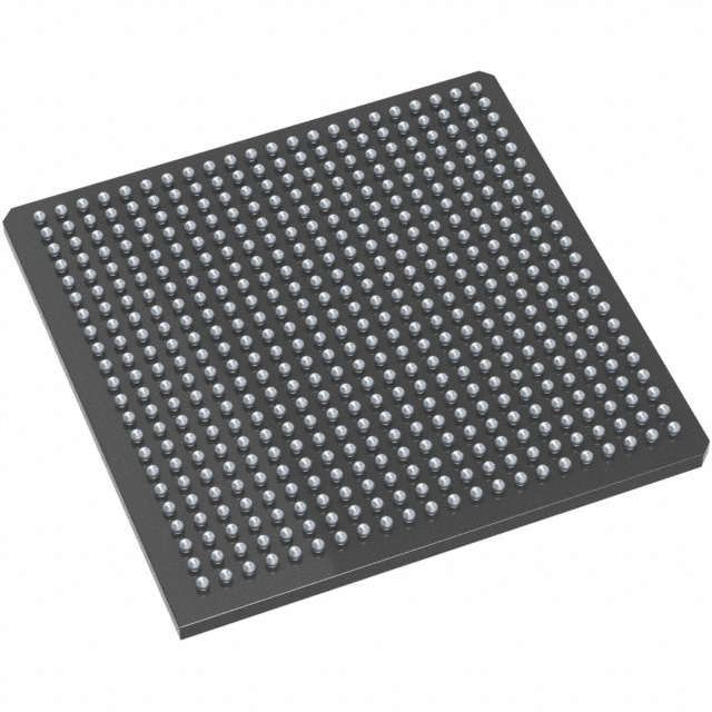
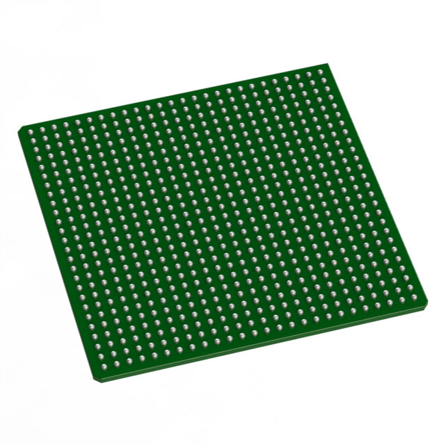
AX1000-1FG484M
| Part Description |
Axcelerator Field Programmable Gate Array (FPGA) IC 317 165888 484-BGA |
|---|---|
| Quantity | 236 Available (as of June 18, 2026) |
| Product Category | Field Programmable Gate Array (FPGA) |
|---|---|
| Manufacturer | Microchip Technology |
| Manufacturing Status | Active |
| Manufacturer Standard Lead Time | 20 Weeks |
| Datasheet |
Specifications & Environmental
| Device Package | 484-FPBGA (23x23) | Grade | Military | Operating Temperature | -55°C – 125°C | ||
|---|---|---|---|---|---|---|---|
| Package / Case | 484-BGA | Number of I/O | 317 | Voltage | 1.425 V - 1.575 V | ||
| Mounting Method | Surface Mount | RoHS Compliance | RoHS non-compliant | REACH Compliance | REACH Unaffected | ||
| Moisture Sensitivity Level | 3 (168 Hours) | Number of LABs/CLBs | 18144 | Number of Logic Elements/Cells | 18144 | ||
| Number of Gates | 1000000 | ECCN | 3A001A2C | HTS Code | 8542.39.0001 | ||
| Qualification | N/A | Total RAM Bits | 165888 |
Overview of AX1000-1FG484M – Axcelerator Field Programmable Gate Array (FPGA) IC 317 165888 484-BGA
The AX1000-1FG484M is an Axcelerator family antifuse FPGA based on Microchip's AX architecture, offering a single-chip, nonvolatile programmable solution. It combines up to 1,000,000 equivalent system gates with 18,144 logic elements and embedded SRAM/FIFO to support complex, high-performance logic implementations.
Designed for military-grade environments, this device supports a wide operating temperature range (−55 °C to 125 °C) and a core voltage range of 1.425 V to 1.575 V. It is targeted at applications that require deterministic timing, on-chip memory and FIFO capabilities, and flexible high-speed I/O options.
Key Features
- Logic Capacity: 1,000,000 equivalent system gates and 18,144 logic elements provide the resources needed for large, complex designs.
- Embedded Memory & FIFOs: Approximately 0.166 Mbits (165,888 bits) of on-chip SRAM with embedded FIFO control logic and variable-aspect RAM blocks for flexible memory organization.
- High-Speed Performance: Family-level performance indicators include 350+ MHz system performance and 500+ MHz internal performance; includes embedded PLLs with 14–200 MHz input range and frequency synthesis capabilities up to 1 GHz.
- Flexible, Multi-Standard I/Os: 317 user I/Os with support for mixed-voltage operation (1.5V, 1.8V, 2.5V, 3.3V), bank-selectable I/Os (8 banks per device family), differential LVDS/LVPECL and common single-ended standards.
- High-Speed Serial Capability: I/Os capable of LVDS operation up to 700 Mb/s for high-throughput interfaces.
- Programmability & I/O Control: Programmable slew rate and drive strength on outputs, programmable input delay and weak pull-up/pull-down options for signal integrity tuning.
- Security & Test: FuseLock™ programming technology and IEEE 1149.1 (JTAG) boundary-scan testing for design protection and manufacturing diagnostics.
- Package & Mounting: 484-ball Fine PBGA (484-FPBGA, 23 × 23) surface-mount package for dense board-level integration.
- Operating Conditions: Military grade with an operating temperature range of −55 °C to 125 °C and a core supply range of 1.425 V to 1.575 V.
Typical Applications
- Defense & Aerospace: Military-grade temperature rating and nonvolatile single-chip antifuse architecture make this FPGA suitable for mission-critical embedded systems and ruggedized electronics.
- High-Speed Data Acquisition: Embedded FIFOs and on-chip SRAM enable efficient buffering and streaming for instrumentation, radar, and high-bandwidth sensor systems.
- Communications & Networking: High-performance PLLs and LVDS-capable I/Os support high-rate serial interfaces and protocol bridging in communication equipment.
- Custom Hardware Acceleration: Large logic capacity and deterministic timing are suitable for offloading compute-critical functions and implementing application-specific accelerators.
Unique Advantages
- Single-Chip Nonvolatile Solution: Antifuse technology provides nonvolatile configuration without external configuration memories, simplifying board design and improving reliability.
- Deterministic Timing and On-Chip PLLs: Segmentable clocks and embedded PLLs enable controlled timing architectures and frequency synthesis for demanding, timing-sensitive designs.
- Flexible I/O Standards: Mixed-voltage support and programmable I/O characteristics reduce the need for level-shifters and external buffering, lowering BOM and board complexity.
- Embedded Memory with FIFO Support: Integrated SRAM blocks and FIFO control logic streamline data buffering and pipeline implementations, minimizing external memory dependencies.
- Security and Testability: FuseLock™ programming and JTAG boundary-scan support help protect IP and simplify manufacturing test flows.
- Rugged, High-Temperature Operation: Military-grade temperature range and surface-mount FPBGA packaging support deployment in harsh environments.
Why Choose AX1000-1FG484M?
The AX1000-1FG484M positions itself as a high-capacity, military-grade antifuse FPGA that combines substantial logic resources, embedded memory/FIFO capability, and flexible high-speed I/O in a single nonvolatile device. Its deterministic timing, integrated PLLs, and programmable I/O controls make it suited for systems that require predictable performance and compact system integration.
This device is appropriate for engineering teams building ruggedized communications, defense, and high-performance embedded systems that demand on-chip memory, robust security features, and a broad set of I/O standards. The combination of integration and configurability helps reduce system BOM and simplifies board-level design while supporting demanding environmental requirements.
Request a quote or submit an inquiry to receive pricing, availability, and lead-time information for the AX1000-1FG484M. Our team can provide assistance with ordering and technical questions to help evaluate this FPGA for your design.


Date Founded: 1989
Headquarters: Chandler, Arizona, USA
Employees: 22,000+
Revenue: $8.349 Billion
Certifications and Memberships: ISO9001:2015, IATF16949:2016, AS 9100D


