
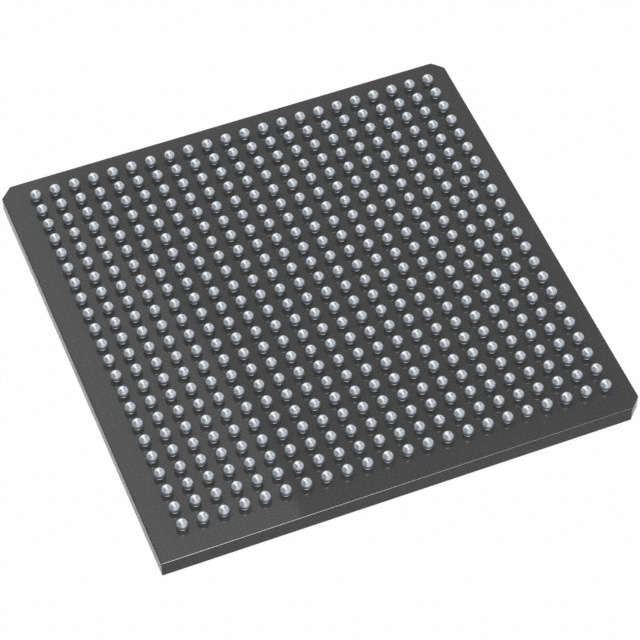
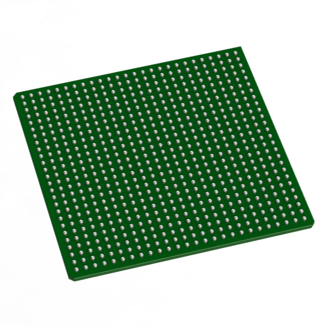
AX1000-1FG484I
| Part Description |
Axcelerator Field Programmable Gate Array (FPGA) IC 317 165888 484-BGA |
|---|---|
| Quantity | 98 Available (as of June 18, 2026) |

| Product Category | Field Programmable Gate Array (FPGA) |
|---|---|
| Manufacturer | Microchip Technology |
| Manufacturing Status | Active |
| Manufacturer Standard Lead Time | 12 Weeks |
| Datasheet |
Specifications & Environmental
| Device Package | 484-FPBGA (23x23) | Grade | Industrial | Operating Temperature | -40°C – 85°C | ||
|---|---|---|---|---|---|---|---|
| Package / Case | 484-BGA | Number of I/O | 317 | Voltage | 1.425 V - 1.575 V | ||
| Mounting Method | Surface Mount | RoHS Compliance | RoHS non-compliant | REACH Compliance | REACH Unaffected | ||
| Moisture Sensitivity Level | 3 (168 Hours) | Number of LABs/CLBs | 18144 | Number of Logic Elements/Cells | 18144 | ||
| Number of Gates | 1000000 | ECCN | 3A001A7A | HTS Code | 8542.39.0001 | ||
| Qualification | N/A | Total RAM Bits | 165888 |
Overview of AX1000-1FG484I – Axcelerator FPGA, 1,000,000 Gates, 484-BGA
The AX1000-1FG484I Axcelerator is a nonvolatile antifuse FPGA built on Microchip Technology’s AX architecture. This industrial-grade, single-chip programmable device delivers high-density logic (1,000,000 equivalent system gates) combined with embedded SRAM and flexible I/O to address demanding embedded and industrial applications that require performance, security and deterministic timing.
Designed for system-level integration, the device provides on-chip memory, PLLs, and multi-standard I/O capability while operating over a 1.425 V to 1.575 V core supply and an industrial temperature range of -40°C to 85°C.
Key Features
- Core Performance 1,000,000 equivalent system gates and 18,144 logic elements provide high combinatorial and registered resource density for complex logic implementations.
- Embedded Memory Approximately 0.166 Mbits of embedded memory (165,888 total RAM bits) implemented across the device to support FIFOs and on-chip storage.
- I/O and Interface Flexibility 317 user I/O pins on this device with series-level support for multi-voltage operation (1.5 V, 1.8 V, 2.5 V, 3.3 V), differential standards (LVDS, LVPECL) and programmable drive/slew options for diverse interface requirements.
- High-Speed and Timing Series-level capabilities include 350+ MHz system performance and 500+ MHz internal performance, segmentable clocks and embedded PLLs (14–200 MHz input range, frequency synthesis up to 1 GHz) for deterministic, high-speed designs.
- Security and Nonvolatile Programming Antifuse-based single-chip, nonvolatile architecture with FuseLock programming technology to protect designs from reverse engineering and unauthorized access.
- Package and Mechanical 484-ball fine-pitch BGA (484-FPBGA, 23×23) surface-mount package for high-density board integration.
- Industrial Reliability Industrial temperature grade (-40°C to 85°C) and RoHS-compliant manufacturing for deployment in industrial environments.
Typical Applications
- Industrial Control and Automation Implement complex control logic, sequencing, and protocol bridging with deterministic timing and industrial temperature support.
- High-Speed Data Path and Interface Bridging Use embedded FIFOs, PLLs and multi-standard I/Os to manage high-speed serial links and data buffering between subsystems.
- Secure Hardware Implementations Leverage antifuse nonvolatile programming and FuseLock protection to safeguard intellectual property in security-sensitive designs.
Unique Advantages
- High-density programmable logic: 1,000,000 equivalent gates and 18,144 logic elements enable compact implementation of large logic functions on a single chip, reducing board-level BOM.
- On-chip memory and FIFO support: Approximately 0.166 Mbits of embedded SRAM with FIFO control logic simplifies data buffering and stream handling without external memory.
- Flexible I/O standards: Bank-selectable, mixed-voltage and differential I/O support allows integration with a wide range of legacy and modern interfaces.
- Deterministic timing and PLLs: Segmentable clocks and integrated PLLs provide stable, user-controllable timing for latency-sensitive applications.
- Design security: Antifuse-based nonvolatile programming and FuseLock protect designs against reverse engineering and tampering.
- Industrial-grade robustness: Specified for -40°C to 85°C operation and RoHS compliance for long-term reliability in industrial deployments.
Why Choose AX1000-1FG484I?
The AX1000-1FG484I offers a balance of high logic capacity, embedded memory and flexible I/O in a nonvolatile antifuse FPGA tailored for industrial applications. Its AX architecture delivers system-level features—PLLs, segmentable clocks and embedded FIFOs—while providing design protection through FuseLock technology.
This device is well suited for engineers building robust, secure, and high-performance embedded systems where deterministic timing, on-chip memory and industrial temperature operation are required. The combination of resources and series-level performance features provides a scalable path within the Axcelerator family for evolving product requirements.
Request a quote or submit an inquiry to obtain pricing and availability for AX1000-1FG484I and to discuss integration details for your design.


Date Founded: 1989
Headquarters: Chandler, Arizona, USA
Employees: 22,000+
Revenue: $8.349 Billion
Certifications and Memberships: ISO9001:2015, IATF16949:2016, AS 9100D


