
AX1000-1BGG729M
| Part Description |
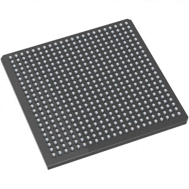
Axcelerator Field Programmable Gate Array (FPGA) IC 516 165888 729-BBGA |
|---|---|
| Quantity | 587 Available (as of June 15, 2026) |

| Product Category | Field Programmable Gate Array (FPGA) |
|---|---|
| Manufacturer | Microchip Technology |
| Manufacturing Status | Active |
| Manufacturer Standard Lead Time | 52 Weeks |
| Datasheet |
Specifications & Environmental
| Device Package | 729-PBGA (35x35) | Grade | Military | Operating Temperature | -55°C – 125°C | ||
|---|---|---|---|---|---|---|---|
| Package / Case | 729-BBGA | Number of I/O | 516 | Voltage | 1.425 V - 1.575 V | ||
| Mounting Method | Surface Mount | RoHS Compliance | ROHS3 Compliant | REACH Compliance | REACH Unaffected | ||
| Moisture Sensitivity Level | 3 (168 Hours) | Number of LABs/CLBs | 18144 | Number of Logic Elements/Cells | 18144 | ||
| Number of Gates | 1000000 | ECCN | 3A001A2C | HTS Code | 8542.39.0001 | ||
| Qualification | N/A | Total RAM Bits | 165888 |
Overview of AX1000-1BGG729M – Axcelerator FPGA, 516 I/O, ~165,888‑bit Embedded RAM, 729‑BBGA
The AX1000-1BGG729M is an Axcelerator family antifuse Field Programmable Gate Array (FPGA) from Microchip Technology using the AX architecture. It provides a nonvolatile, single‑chip solution with on‑chip embedded SRAM/FIFO, segmentable clocks, and integrated PLLs for system-level designs that require deterministic timing and design security.
With 1,000,000 equivalent system gates, 516 user I/Os and approximately 165,888 bits of embedded memory, this device is suited for high‑performance, security‑sensitive and military‑grade applications where robustness across a wide temperature range is required.
Key Features
- Core Architecture — AX antifuse architecture implemented in a CMOS 0.15 µm process with seven metal layers; provides nonvolatile single‑chip configuration and FuseLock programming technology for design protection.
- Logic Capacity — Approximately 1,000,000 equivalent system gates and 18,144 logic elements, enabling complex system integration on a single device.
- Embedded Memory & FIFOs — Around 165,888 bits of embedded SRAM organized in 36 core RAM blocks with embedded FIFO control logic for high‑performance buffering and dataflow control.
- I/O Flexibility — 516 user I/Os with bank‑selectable, multi‑standard support and LVDS capability up to 700 Mb/s; programmable slew rate, drive strength and input pull options.
- Clocking & PLLs — Segmentable clock resources and an embedded PLL family capability with 14–200 MHz input range and frequency synthesis up to 1 GHz for precise timing and clock generation.
- Performance — Family‑level performance specifications include 350+ MHz system performance and 500+ MHz internal performance for demanding logic and signal processing tasks.
- Package & Mounting — 729‑BBGA package (supplier package: 729‑PBGA, 35 × 35 mm) with surface‑mount mounting type suitable for high‑density board designs.
- Power & Environmental — Core supply voltage range 1.425 V to 1.575 V; operating temperature range −55 °C to 125 °C; RoHS‑compliant. Grade: Military.
Typical Applications
- Military and Defense Systems — Military grade temperature range and nonvolatile antifuse security features make the device suitable for rugged, security‑sensitive military electronics and communications equipment.
- High‑Performance Signal Processing — Large logic capacity, high internal operating speeds and embedded FIFOs support FPGA‑based signal processing and real‑time data pipelines.
- Secure, One‑Time Programmable Designs — Antifuse technology combined with FuseLock provides protection against reverse engineering for one‑time programmable, secure applications.
- Complex Embedded Controllers — Abundant I/Os, on‑chip RAM and multiple clock domains enable integration of control logic, I/O aggregation and system glue logic on a single device.
Unique Advantages
- Nonvolatile, Secure Configuration: Antifuse programming and FuseLock technology protect IP and prevent device cloning or reverse engineering.
- High Integration Density: One million equivalent system gates and 18,144 logic elements reduce external glue logic and simplify board-level design.
- Deterministic Timing and Clocking: Segmentable clocks and embedded PLLs with wide input range allow precise, predictable timing for real‑time systems.
- Embedded Memory with FIFO Support: Approximately 165,888 bits of RAM and FIFO control logic simplify buffering and high‑throughput data handling without external memory.
- Rugged Operating Range: −55 °C to 125 °C operating temperature and military classification address demanding environmental requirements.
- Flexible I/O Standards: Bank‑selectable multi‑voltage I/Os and high‑speed LVDS capability support diverse interface requirements and mixed‑voltage systems.
Why Choose AX1000-1BGG729M?
The AX1000-1BGG729M combines antifuse nonvolatile security, high logic density and substantial embedded memory in a single, military‑grade FPGA. Its AX architecture and integrated system features (clock segmentation, PLLs, embedded FIFOs) make it a practical choice for designers who need deterministic performance, on‑chip buffering and hardened IP protection.
This device is well suited to designers building secure, high‑performance and rugged systems that require long‑term stability, high integration and the ability to implement complex logic and high‑speed I/O on a single package.
Request a quote or submit an inquiry to discuss availability, lead times and pricing for the AX1000-1BGG729M. Our team can provide product ordering information and support for your design evaluation and deployment needs.


Date Founded: 1989
Headquarters: Chandler, Arizona, USA
Employees: 22,000+
Revenue: $8.349 Billion
Certifications and Memberships: ISO9001:2015, IATF16949:2016, AS 9100D


