
AX1000-1BGG729I
| Part Description |
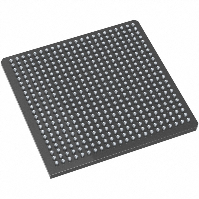
Axcelerator Field Programmable Gate Array (FPGA) IC 516 165888 729-BBGA |
|---|---|
| Quantity | 1,506 Available (as of June 18, 2026) |

| Product Category | Field Programmable Gate Array (FPGA) |
|---|---|
| Manufacturer | Microchip Technology |
| Manufacturing Status | Active |
| Manufacturer Standard Lead Time | 52 Weeks |
| Datasheet |
Specifications & Environmental
| Device Package | 729-PBGA (35x35) | Grade | Industrial | Operating Temperature | -40°C – 85°C | ||
|---|---|---|---|---|---|---|---|
| Package / Case | 729-BBGA | Number of I/O | 516 | Voltage | 1.425 V - 1.575 V | ||
| Mounting Method | Surface Mount | RoHS Compliance | ROHS3 Compliant | REACH Compliance | REACH Unaffected | ||
| Moisture Sensitivity Level | 3 (168 Hours) | Number of LABs/CLBs | 18144 | Number of Logic Elements/Cells | 18144 | ||
| Number of Gates | 1000000 | ECCN | 3A001A7A | HTS Code | 8542.39.0001 | ||
| Qualification | N/A | Total RAM Bits | 165888 |
Overview of AX1000-1BGG729I – Axcelerator Field Programmable Gate Array (FPGA) IC, 516 I/Os, 165,888‑bit RAM, 729‑BBGA
The AX1000-1BGG729I is an Axcelerator family FPGA from Microchip Technology implementing the AX architecture and antifuse programming technology. It delivers a single-chip, nonvolatile FPGA solution with deterministic timing and on-chip embedded memory, intended for designs that require high-performance, secure, and reliable logic integration.
This device combines high logic capacity, substantial embedded RAM, and a large I/O count in a 729‑ball BGA package for industrial applications that demand robust temperature range and board-level integration.
Key Features
- Core Capacity — Approximately 1,000,000 equivalent system gates with 18,144 logic elements for complex logic integration.
- Embedded Memory — Approximately 0.166 Mbits (165,888 bits) of on-chip RAM arranged as 36 core RAM blocks with embedded FIFO control logic for buffering and data handling.
- I/O and Interfaces — 516 user I/Os; I/O standards include multi-voltage operation and high-speed differential options noted in the Axcelerator family (LVDS-capable up to 700 Mb/s).
- Performance — Family-level performance characteristics include 350+ MHz system performance and 500+ MHz internal performance, with on-chip PLLs and segmentable clock resources for flexible clocking.
- Power and Voltage — Core supply range 1.425 V to 1.575 V (nominal 1.5 V core voltage for low-power operation).
- Packaging and Mounting — Surface-mount 729‑BBGA package (supplier package listed as 729‑PBGA, 35×35 mm) for compact board implementation.
- Industrial Grade and Temperature — Industrial operating temperature range of −40 °C to 85 °C.
- Security and Test — Family features include FuseLock™ programming to protect design IP, boundary-scan (IEEE 1149.1) support, and in-system diagnostic/debug capability with Microchip Silicon Explorer II.
- Standards and Compliance — RoHS-compliant.
Typical Applications
- High-speed data interfaces — Use the device’s LVDS-capable I/Os and embedded FIFOs to implement multi-gigabit interface buffering and protocol bridging.
- Deterministic control logic — Leverage deterministic, user-controllable timing and segmentable clocks for timing-critical control and real-time processing functions.
- Secure, single-chip implementations — Deploy the antifuse, nonvolatile fabric and FuseLock programming to protect IP in applications that need built-in security and nonvolatile configuration.
- Memory-intensive logic — Use the 36 embedded RAM blocks and FIFO control logic for packet buffering, data queuing, and width-adaptable memory structures.
Unique Advantages
- Single-chip nonvolatile solution: Eliminates external configuration memory and delivers instant, secure configuration at power-up.
- High logic and I/O density: 1,000,000 equivalent gates and 516 user I/Os support complex designs and extensive board-level interfacing without multiple devices.
- Embedded FIFO and RAM flexibility: Width-configurable embedded RAM blocks and programmable FIFO control logic simplify data buffering and interface width adaptation.
- Deterministic timing and clocking: Segmentable clock resources and embedded PLLs provide controllable, high-performance clocking for timing-sensitive applications.
- Design security and testability: FuseLock programming, boundary-scan compliance, and in-system diagnostic capability help protect IP and streamline production test and debugging.
- Industrial robustness: Industrial temperature rating (−40 °C to 85 °C) and RoHS compliance for deployment in regulated environments.
Why Choose AX1000-1BGG729I?
The AX1000-1BGG729I offers a balanced combination of high gate count, substantial embedded memory, and a large I/O set within a compact 729‑BBGA package—suitable for engineers who need a secure, nonvolatile FPGA platform with deterministic performance. Its family-proven architecture provides PLLs, segmentable clocks, and embedded FIFOs to address timing-critical and data-intensive designs.
Backed by Axcelerator family features such as FuseLock programming, boundary-scan testability, and in-system diagnostic support, the AX1000-1BGG729I is positioned for long-term integration where security, reliability, and predictable timing matter.
Request a quote or submit an inquiry to confirm pricing, availability, and lead times for AX1000-1BGG729I. Our team can provide technical information and ordering support tailored to your project needs.


Date Founded: 1989
Headquarters: Chandler, Arizona, USA
Employees: 22,000+
Revenue: $8.349 Billion
Certifications and Memberships: ISO9001:2015, IATF16949:2016, AS 9100D


