
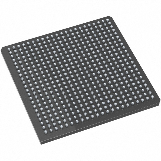
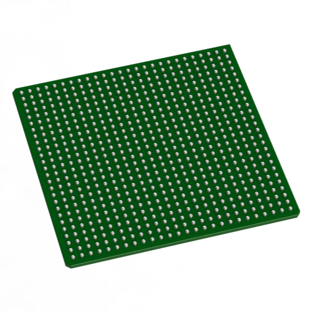
AX1000-1FG896M
| Part Description |
Axcelerator Field Programmable Gate Array (FPGA) IC 516 165888 896-BGA |
|---|---|
| Quantity | 660 Available (as of June 18, 2026) |

| Product Category | Field Programmable Gate Array (FPGA) |
|---|---|
| Manufacturer | Microchip Technology |
| Manufacturing Status | Active |
| Manufacturer Standard Lead Time | 20 Weeks |
| Datasheet |
Specifications & Environmental
| Device Package | 896-FBGA (31x31) | Grade | Military | Operating Temperature | -55°C – 125°C | ||
|---|---|---|---|---|---|---|---|
| Package / Case | 896-BGA | Number of I/O | 516 | Voltage | 1.425 V - 1.575 V | ||
| Mounting Method | Surface Mount | RoHS Compliance | RoHS non-compliant | REACH Compliance | REACH Unaffected | ||
| Moisture Sensitivity Level | 3 (168 Hours) | Number of LABs/CLBs | 18144 | Number of Logic Elements/Cells | 18144 | ||
| Number of Gates | 1000000 | ECCN | 3A001A2C | HTS Code | 8542.39.0001 | ||
| Qualification | N/A | Total RAM Bits | 165888 |
Overview of AX1000-1FG896M – Axcelerator FPGA, 1,000,000 gates, 516 I/Os, 896-BGA
The AX1000-1FG896M is an Axcelerator family field-programmable gate array (FPGA) by Microchip Technology built on the AX antifuse architecture. It delivers a one-million-equivalent-system-gate capacity with 18,144 logic elements and rich on-chip resources to support high-performance, secure programmable logic designs.
Designed for applications that require high I/O density, deterministic timing and nonvolatile configuration, this military-grade device provides a compact 896-BGA footprint, broad I/O flexibility and an extended operating range for use in demanding environments.
Key Features
- Core Logic Approximately 1,000,000 equivalent system gates and 18,144 logic elements provide substantial programmable logic capacity for complex designs.
- Embedded Memory & FIFOs Approximately 0.166 Mbits (165,888 bits) of on-chip RAM with embedded FIFO control logic and variable-aspect RAM blocks for width-configurable read/write ports.
- I/O Flexibility 516 user I/Os with bank-selectable, mixed-voltage operation (1.5V, 1.8V, 2.5V, 3.3V) and support for single-ended and differential standards, including LVDS capability up to 700 Mb/s.
- Clocking & PLLs Segmentable clock resources and embedded phase-locked loop functionality (14–200 MHz input range with frequency synthesis capability up to 1 GHz) for flexible clock management.
- Power & Supply Core voltage supply nominally centered around 1.5 V (specified 1.425 V to 1.575 V) to match low-voltage FPGA system architectures.
- Package & Mounting 896-ball fine BGA (896-FBGA, 31×31) in a surface-mount package for high density board-level integration.
- Reliability & Security Single-chip, nonvolatile antifuse programming with FuseLock™ programming technology to protect designs against reverse engineering and enable deterministic, user-controllable timing.
- Operational Range Military-grade temperature specification from −55 °C to +125 °C for deployment in harsh environments.
Typical Applications
- Military & Aerospace Systems High-density, military-grade FPGA for signal processing, protocol bridging and mission-critical logic in extreme temperature environments.
- High-Speed Data Interfaces LVDS-capable I/Os and embedded FIFOs suit high-throughput serial interfaces, data aggregation and real-time data buffering.
- Secure and Protected Designs Antifuse-based nonvolatile configuration and FuseLock™ security help protect intellectual property and enable tamper-resistant implementations.
- Communications & Networking Large logic capacity and extensive I/O count enable complex packet processing, protocol offload and custom switching functions.
Unique Advantages
- High Logic Density: 1,000,000 equivalent gates and 18,144 logic elements allow consolidation of complex functions into a single device, reducing system board count.
- Nonvolatile, Tamper-Resistant Configuration: Antifuse architecture with FuseLock™ secures designs and removes the need for external configuration memory.
- Flexible, High-Speed I/O: 516 I/Os with multi-standard support and LVDS capability provide versatile interfacing for a wide range of sensors, transceivers and backplane connections.
- Deterministic Timing & On-Chip Clocking: Segmentable clock resources and embedded PLLs enable precise, controllable timing for latency-sensitive designs.
- Wide Thermal Range: Specified operation from −55 °C to +125 °C supports deployment in harsh or temperature-extreme environments.
- Compact, High-Density Package: 896-FBGA (31×31) surface-mount package optimizes board area while providing abundant I/O.
Why Choose AX1000-1FG896M?
The AX1000-1FG896M positions itself as a high-capacity, secure and rugged FPGA solution for designs that demand substantial logic resources, broad I/O capability and nonvolatile configuration. Its combination of one million equivalent gates, extensive embedded memory/FIFO support and military-grade temperature range makes it well suited to applications where performance and reliability are essential.
Engineers building complex signal processing, secure communications or mission-critical control systems will benefit from the device's deterministic timing, on-chip PLLs and comprehensive I/O standards—enabling system consolidation, reduced BOM and long-term deployment stability.
Request a quote or submit an inquiry to receive pricing, lead-time and availability information for the AX1000-1FG896M.


Date Founded: 1989
Headquarters: Chandler, Arizona, USA
Employees: 22,000+
Revenue: $8.349 Billion
Certifications and Memberships: ISO9001:2015, IATF16949:2016, AS 9100D


