
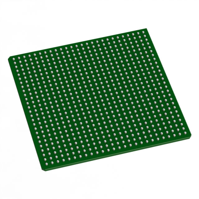
AX1000-1FGG676
| Part Description |
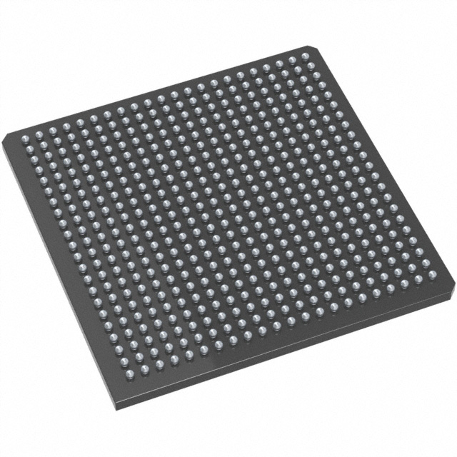
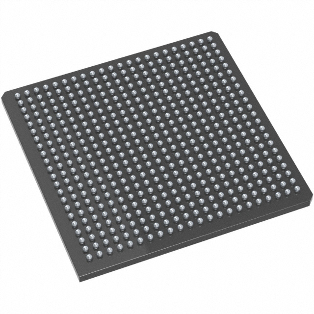
Axcelerator Field Programmable Gate Array (FPGA) IC 418 165888 676-BGA |
|---|---|
| Quantity | 1,451 Available (as of October 8, 2026) |
| Product Category | Field Programmable Gate Array (FPGA) |
|---|---|
| Manufacturer | Microchip Technology |
| Manufacturing Status | Active |
| Manufacturer Standard Lead Time | 12 Weeks |
| Datasheet |
Specifications & Environmental
| Device Package | 676-FBGA (27x27) | Grade | Commercial | Operating Temperature | 0°C – 70°C | ||
|---|---|---|---|---|---|---|---|
| Package / Case | 676-BGA | Number of I/O | 418 | Voltage | 1.425 V - 1.575 V | ||
| Mounting Method | Surface Mount | RoHS Compliance | ROHS3 Compliant | REACH Compliance | REACH Unaffected | ||
| Moisture Sensitivity Level | 3 (168 Hours) | Number of LABs/CLBs | 18144 | Number of Logic Elements/Cells | 18144 | ||
| Number of Gates | 1000000 | ECCN | 3A001A7A | HTS Code | 8542.39.0001 | ||
| Qualification | N/A | Total RAM Bits | 165888 |
Overview of AX1000-1FGG676 – Axcelerator Field Programmable Gate Array (FPGA) IC, 418 I/Os, 165,888 bits, 676-BGA
The AX1000-1FGG676 is a commercial-grade Axcelerator FPGA from Microchip Technology that implements the AX antifuse architecture for a single-chip, nonvolatile solution. This device delivers up to 1,000,000 equivalent system gates with 18,144 logic elements and approximately 0.166 Mbits of embedded RAM, making it suitable for high-performance digital designs requiring dense logic, on-chip memory, and flexible I/O.
Built with system-level capabilities from the Axcelerator family, the part targets applications that require deterministic timing, embedded FIFO memory control, and multi-standard I/O support while operating within a 0 °C to 70 °C commercial temperature range and a 1.425 V to 1.575 V core supply window.
Key Features
- Core Capacity — Approximately 1,000,000 equivalent system gates and 18,144 logic elements provide substantial programmable logic resources for complex designs.
- Embedded Memory — Total on-chip RAM of 165,888 bits (approximately 0.166 Mbits) with embedded FIFO control logic for buffering and data-stream management.
- I/O Flexibility — 418 user I/Os supporting mixed-voltage operation and a wide range of single-ended and differential interfaces as described for the Axcelerator family.
- Performance and Timing — Family-specified performance characteristics include high internal and system performance, deterministic and user-controllable timing, segmentable clock resources, and integrated PLLs for frequency synthesis and clock management.
- Security and Nonvolatile Configuration — Antifuse-based, single-chip nonvolatile programming with FuseLock™ programming technology to protect against reverse engineering and design theft.
- Package & Mounting — 676-ball fine-pitch BGA (676-FBGA, 27 × 27) in a surface-mount form factor; commercial-grade temperature rating (0 °C to 70 °C).
- Power — Core supply range of 1.425 V to 1.575 V for compatible power-rail design and low-voltage operation.
- Standards & Tools — Boundary-scan (JTAG) support and unique in-system diagnostic/debug capability with Microchip Silicon Explorer II, as provided by the Axcelerator family documentation.
- Compliance — RoHS compliant.
Typical Applications
- High-Speed Data Interfaces — Implement LVDS and other differential interfaces and use embedded FIFOs for reliable, high-throughput data transfer and buffering.
- Networking and Telecom Modules — Use the device’s logic density and embedded RAM to implement packet processing, protocol bridging, and interface adaptation in commercial networking equipment.
- Signal Processing and Compute Acceleration — Deploy the logic elements and on-chip memory for real-time processing tasks and hardware-accelerated algorithms in compact, single-chip solutions.
- Security-Sensitive Designs — Leverage antifuse nonvolatile programming and FuseLock technology for designs where configuration protection and intellectual-property security are important.
Unique Advantages
- Single-Chip Nonvolatile Solution: Antifuse architecture removes the need for external configuration memory and simplifies system power-up behavior.
- Deterministic Timing and Clock Control: Segmentable clocks and integrated PLLs provide precise timing control for synchronous systems and frequency synthesis needs.
- Embedded FIFO and Memory Control: On-chip RAM blocks with FIFO control logic reduce external memory requirements and simplify buffer designs for streaming data.
- Design Security: FuseLock programming technology protects configuration data against reverse engineering and unauthorized access.
- High I/O Count in Compact Package: 418 I/Os in a 676-FBGA package enable dense connectivity in space-constrained commercial applications.
- Diagnostic and Debug Support: In-system diagnostic capability with Microchip Silicon Explorer II aids development and troubleshooting.
Why Choose AX1000-1FGG676?
The AX1000-1FGG676 positions itself as a high-density, commercial-grade FPGA offering a balanced combination of logic capacity, embedded memory, and I/O flexibility in a single nonvolatile device. Its antifuse-based configuration and FuseLock protection make it well suited for applications that require secure, deterministic operation with integrated FIFO support and advanced clocking.
This part is ideal for designers building commercial networking, communications, and high-performance embedded systems who need scalable logic resources, on-chip buffering, and robust timing control while operating within standard commercial temperature and supply constraints.
Request a quote or submit an RFQ to receive pricing and lead-time information for the AX1000-1FGG676.





















Date Founded: 1989
Headquarters: Chandler, Arizona, USA
Employees: 22,000+
Revenue: $8.349 Billion
Certifications and Memberships: ISO9001:2015, IATF16949:2016, AS 9100D




