
AX1000-1FGG896M
| Part Description |
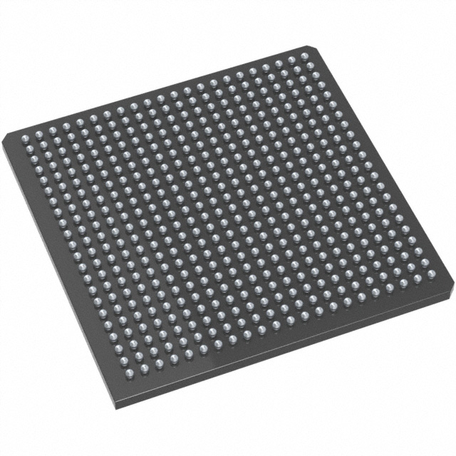
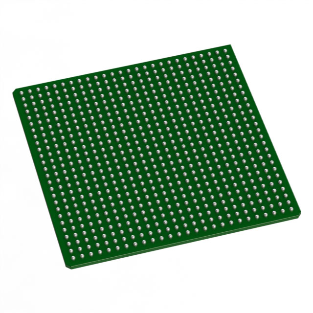
Axcelerator Field Programmable Gate Array (FPGA) IC 516 165888 896-BGA |
|---|---|
| Quantity | 946 Available (as of October 8, 2026) |

| Product Category | Field Programmable Gate Array (FPGA) |
|---|---|
| Manufacturer | Microchip Technology |
| Manufacturing Status | Active |
| Manufacturer Standard Lead Time | 20 Weeks |
| Datasheet |
Specifications & Environmental
| Device Package | 896-FBGA (31x31) | Grade | Military | Operating Temperature | -55°C – 125°C | ||
|---|---|---|---|---|---|---|---|
| Package / Case | 896-BGA | Number of I/O | 516 | Voltage | 1.425 V - 1.575 V | ||
| Mounting Method | Surface Mount | RoHS Compliance | ROHS3 Compliant | REACH Compliance | REACH Unaffected | ||
| Moisture Sensitivity Level | 3 (168 Hours) | Number of LABs/CLBs | 18144 | Number of Logic Elements/Cells | 18144 | ||
| Number of Gates | 1000000 | ECCN | 3A001A2C | HTS Code | 8542.39.0001 | ||
| Qualification | N/A | Total RAM Bits | 165888 |
Overview of AX1000-1FGG896M – Axcelerator Field Programmable Gate Array (FPGA) IC 516 165888 896-BGA
The AX1000-1FGG896M is a member of Microchip Technology’s Axcelerator antifuse FPGA family using the AX architecture. This single-chip, nonvolatile FPGA delivers 1,000,000 equivalent system gates with 18,144 logic elements and embedded memory to support high-performance, security-conscious designs.
Designed for applications that require deterministic timing, embedded FIFOs, and high-speed I/O, the device targets markets where military-grade operating range and on-chip nonvolatile configuration are required. Key value propositions include high internal performance, flexible multi-standard I/Os, and on-chip embedded memory and PLL resources for system-level integration.
Key Features
- Core Capacity — 1,000,000 equivalent system gates and 18,144 logic elements provide substantial logic density for complex functions and system integration.
- Embedded Memory — 165,888 total RAM bits (approximately 0.166 Mbits) organized in configurable RAM/FIFO blocks with embedded FIFO control logic for packet buffering and data staging.
- I/O Resources — 516 user I/Os with support for multi-standard operation including LVDS-capable interfaces (700 Mb/s LVDS capable), differential and single-ended standards, and bank-selectable mixed-voltage operation.
- Performance — Family-level capabilities include 350+ MHz system performance and 500+ MHz internal performance, plus high-performance embedded FIFOs and PLL frequency synthesis capabilities up to 1 GHz.
- Clocking & Timing — Segmentable clock resources and embedded PLLs with a 14–200 MHz input range allow flexible clock management and deterministic, user-controllable timing.
- Nonvolatile Security — Antifuse, single-chip nonvolatile architecture with FuseLock programming technology to help protect design IP and resist reverse engineering.
- Package & Mounting — Surface-mount 896-BGA package; supplier device package listed as 896-FBGA (31×31), suitable for high-density board integration.
- Supply & Temperature — Core voltage supply range 1.425 V to 1.575 V and military-grade operating temperature from −55 °C to 125 °C for deployment in demanding environments.
- Standards & Testability — Boundary-scan (JTAG) support for board-level test and in-system diagnostic and debug capability with Microchip Silicon Explorer II.
Typical Applications
- Military and Defense Systems — Military-grade temperature range (−55 °C to 125 °C) and nonvolatile antifuse architecture with FuseLock provide a secure, rugged solution for defense electronics.
- High-Speed Data Interfaces — LVDS-capable I/Os and embedded FIFOs support high-throughput serial links and data acquisition buffering at hundreds of megabits per second.
- Deterministic Embedded Systems — Segmentable clock resources, embedded PLLs, and deterministic timing make the device suitable for real-time processing and control applications that require predictable latency.
- System Integration and IP Protection — Single-chip nonvolatile configuration reduces external boot components and FuseLock technology helps protect proprietary logic and designs.
Unique Advantages
- High Logic Density: One million equivalent gates and 18,144 logic elements enable consolidation of multiple functions onto a single FPGA, reducing board-level complexity.
- Embedded Memory & FIFOs: Approximately 0.166 Mbits of on-chip RAM with programmable FIFO control improves data buffering and reduces dependence on external memory.
- Multi-Standard I/O Flexibility: Bank-selectable mixed-voltage I/Os and support for differential standards such as LVDS enable interfacing with a wide range of peripherals and link technologies.
- Nonvolatile, Secure Configuration: Antifuse technology and FuseLock programming protect designs against reverse engineering while eliminating configuration storage requirements at power-up.
- Rugged Operating Range: Military-grade temperature specification (−55 °C to 125 °C) expands suitability for harsh-environment deployments.
- Deterministic Timing and Clocking: Segmentable clocks and embedded PLLs provide precise clock management for timing-critical system designs.
Why Choose AX1000-1FGG896M?
AX1000-1FGG896M combines high gate count, substantial logic element capacity, and embedded RAM/FIFO resources in a single, nonvolatile antifuse FPGA tailored for secure, high-performance systems. Its multi-standard I/O flexibility and deterministic clocking features make it a practical choice for designs that require high-throughput interfaces and controlled timing behavior.
This device is well suited to customers building rugged, secure systems who need on-chip memory, embedded clocking and PLLs, and military-grade temperature performance. The Axcelerator architecture and FuseLock programming technology provide long-term robustness and IP protection for deployed designs.
Request a quote or submit an inquiry to discuss availability, pricing, and integration support for AX1000-1FGG896M. Our team can provide technical details and assist with qualification and procurement steps.




















Date Founded: 1989
Headquarters: Chandler, Arizona, USA
Employees: 22,000+
Revenue: $8.349 Billion
Certifications and Memberships: ISO9001:2015, IATF16949:2016, AS 9100D




