
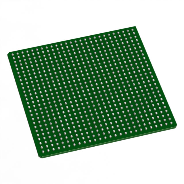
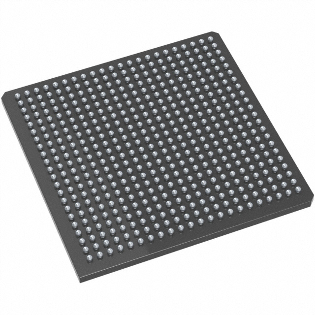
AX1000-2BG729I
| Part Description |
Axcelerator Field Programmable Gate Array (FPGA) IC 516 165888 729-BBGA |
|---|---|
| Quantity | 844 Available (as of June 15, 2026) |

| Product Category | Field Programmable Gate Array (FPGA) |
|---|---|
| Manufacturer | Microchip Technology |
| Manufacturing Status | Active |
| Manufacturer Standard Lead Time | 52 Weeks |
| Datasheet |
Specifications & Environmental
| Device Package | 729-PBGA (35x35) | Grade | Industrial | Operating Temperature | -40°C – 85°C | ||
|---|---|---|---|---|---|---|---|
| Package / Case | 729-BBGA | Number of I/O | 516 | Voltage | 1.425 V - 1.575 V | ||
| Mounting Method | Surface Mount | RoHS Compliance | RoHS non-compliant | REACH Compliance | REACH Unaffected | ||
| Moisture Sensitivity Level | 3 (168 Hours) | Number of LABs/CLBs | 18144 | Number of Logic Elements/Cells | 18144 | ||
| Number of Gates | 1000000 | ECCN | 3A001A7A | HTS Code | 8542.39.0001 | ||
| Qualification | N/A | Total RAM Bits | 165888 |
Overview of AX1000-2BG729I – Axcelerator Field Programmable Gate Array, 516 I/Os, 729-BBGA
The AX1000-2BG729I is an Axcelerator antifuse FPGA from Microchip Technology based on the AX architecture. It delivers a high-density, single-chip, nonvolatile FPGA solution featuring approximately 1,000,000 equivalent system gates and 18,144 logic elements suitable for demanding industrial designs.
Designed for applications that require high I/O count, on-chip embedded memory and deterministic timing, the device combines segmentable clocks, embedded PLLs, high-performance FIFOs and mixed-voltage I/O flexibility to support communications, industrial control and high-performance embedded systems.
Key Features
- Core & Architecture Antifuse-based AX architecture providing a single-chip, nonvolatile FPGA solution optimized for security and deterministic timing.
- Logic Capacity Approximately 1,000,000 equivalent system gates and 18,144 logic elements, enabling complex logic integration on a single device.
- Embedded Memory Approximately 0.166 Mbits (165,888 bits) of embedded RAM/FIFO with variable-aspect 4,608-bit RAM blocks and programmable FIFO control logic.
- I/O & Interfaces 516 user I/Os with bank-selectable, mixed-voltage operation (1.5V, 1.8V, 2.5V, 3.3V) and support for single-ended standards (LVTTL/LVCMOS/PCI) and differential standards including LVDS and LVPECL; LVDS-capable I/Os up to 700 Mb/s.
- Performance Family-level published performance indicators include 350+ MHz system performance and 500+ MHz internal performance, supported by embedded high-performance FIFOs and on-chip PLLs.
- Clocking & Timing Segmentable clock resources and embedded PLLs with a 14–200 MHz input range and frequency synthesis capability up to 1 GHz for flexible clock management.
- Power & Supply Core voltage range of 1.425 V to 1.575 V for low-power operation and mixed-voltage I/O banks for flexible system interfacing.
- Package & Thermal Surface-mount 729-BBGA (supplier package: 729-PBGA, 35×35) designed for industrial-grade operation from -40°C to +85°C.
- Security & Test Nonvolatile antifuse programming with FuseLock programming technology and IEEE 1149.1 (JTAG) boundary-scan support for production test and IP protection.
- Compliance RoHS compliant.
Typical Applications
- Industrial Control — Deterministic timing, high I/O count and industrial temperature range make the AX1000-2BG729I suitable for machine control, motion control and factory automation systems.
- Data Communications — High-performance embedded FIFOs, PLLs and LVDS-capable I/Os support packet buffering, SERDES front-ends and high-speed link interfacing in networking equipment.
- Signal Processing — Large logic capacity and on-chip SRAM are well suited for real-time data processing, video pre-processing and sensor fusion tasks.
- Test & Measurement — Boundary-scan support, deterministic timing and flexible I/O standards facilitate precision measurement systems and instrumentation.
Unique Advantages
- Single-chip nonvolatile solution: Antifuse technology provides one-time programmable, nonvolatile configuration for secure, field-deployed systems without external configuration memory.
- High-density logic and memory: Around 1,000,000 equivalent gates and approximately 0.166 Mbits of embedded RAM enable consolidation of complex functions and buffering on a single device.
- Flexible mixed-voltage I/O: Bank-selectable I/O standards and support for multiple voltage domains simplify integration with diverse system peripherals and legacy interfaces.
- Deterministic timing and clocking: Segmentable clocks and integrated PLLs provide predictable timing and frequency synthesis for latency-sensitive designs.
- Industrial-grade reliability: Qualified for operation from -40°C to +85°C and supplied in a robust 729-BBGA surface-mount package for reliable deployment in industrial environments.
- Production and security features: JTAG boundary-scan and FuseLock programming technology help secure intellectual property and streamline production test flows.
Why Choose AX1000-2BG729I?
The AX1000-2BG729I positions itself as a high-capacity, industrial-grade antifuse FPGA that combines substantial logic and embedded memory with versatile, high-speed I/O options. Its AX architecture and family-level performance characteristics target applications that need deterministic timing, secure nonvolatile configuration and consolidated system integration.
This device is ideal for engineering teams building robust industrial, communications or signal-processing products that require high I/O density, embedded FIFOs and flexible clocking. The combination of on-chip memory, PLLs and mixed-voltage I/Os delivers long-term value through reduced board complexity and simplified system design.
Request a quote or submit an inquiry to start procurement or to receive pricing and availability information for the AX1000-2BG729I.


Date Founded: 1989
Headquarters: Chandler, Arizona, USA
Employees: 22,000+
Revenue: $8.349 Billion
Certifications and Memberships: ISO9001:2015, IATF16949:2016, AS 9100D


