
AX1000-2BG729
| Part Description |
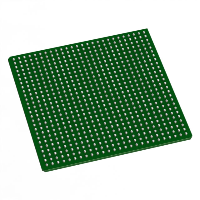
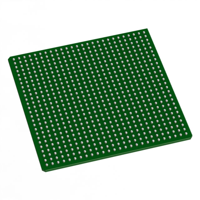
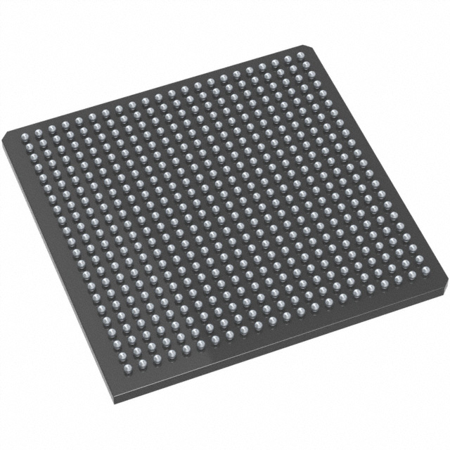
Axcelerator Field Programmable Gate Array (FPGA) IC 516 165888 729-BBGA |
|---|---|
| Quantity | 827 Available (as of October 8, 2026) |

| Product Category | Field Programmable Gate Array (FPGA) |
|---|---|
| Manufacturer | Microchip Technology |
| Manufacturing Status | Active |
| Manufacturer Standard Lead Time | 52 Weeks |
| Datasheet |
Specifications & Environmental
| Device Package | 729-PBGA (35x35) | Grade | Commercial | Operating Temperature | 0°C – 70°C | ||
|---|---|---|---|---|---|---|---|
| Package / Case | 729-BBGA | Number of I/O | 516 | Voltage | 1.425 V - 1.575 V | ||
| Mounting Method | Surface Mount | RoHS Compliance | RoHS non-compliant | REACH Compliance | REACH Unaffected | ||
| Moisture Sensitivity Level | 3 (168 Hours) | Number of LABs/CLBs | 18144 | Number of Logic Elements/Cells | 18144 | ||
| Number of Gates | 1000000 | ECCN | 3A001A7A | HTS Code | 8542.39.0001 | ||
| Qualification | N/A | Total RAM Bits | 165888 |
Overview of AX1000-2BG729 – Axcelerator Field Programmable Gate Array (FPGA) IC 516 165888 729-BBGA
The AX1000-2BG729 from Microchip Technology is an Axcelerator family antifuse FPGA built on the AX architecture, delivering a single-chip, nonvolatile programmable solution targeted at high-performance embedded and system-level designs. The device combines antifuse nonvolatility, segmentable clocks, embedded SRAM with FIFO control logic and on-chip PLLs to serve applications requiring high throughput, deterministic timing and secure programming.
Key value comes from its 1,000,000 equivalent system gates, 18,144 logic elements and approximately 0.166 Mbits of embedded memory, together with 516 user I/Os and a 729-ball BGA package—making it suitable for dense, performance-focused commercial applications where board space, integration and predictable timing matter.
Key Features
- Core architecture and process AX antifuse architecture manufactured on advanced 0.15 µm CMOS antifuse process with seven metal layers, providing a nonvolatile single-chip solution and design security through FuseLock programming.
- Logic resources 18,144 logic elements (as specified) delivering a capacity of 1,000,000 equivalent system gates for complex combinatorial and sequential logic implementations.
- Embedded memory and FIFO Approximately 0.166 Mbits (165,888 bits) of embedded SRAM with programmable FIFO control logic and variable-aspect RAM blocks for width-configurable read/write ports.
- I/O flexibility 516 user I/Os with support for multi-standard, bank-selectable operation and high-speed differential signaling capability (LVDS-capable I/Os), enabling mixed-voltage interfacing across I/O banks.
- Clocking and PLLs Segmentable clock resources and on-chip PLLs provide deterministic, user-controllable timing and frequency synthesis for complex clocking schemes.
- Power and supply Core operating supply range specified at 1.425 V to 1.575 V (nominal 1.5 V), optimized for low-power core operation consistent with antifuse devices.
- Package and mounting Supplied in a 729-BBGA package (supplier package 729-PBGA, 35 × 35 mm), surface-mount mount style suitable for compact, high-density assemblies.
- Commercial grade and compliance Commercial temperature grade with operating range 0 °C to 70 °C and RoHS-compliant status.
Typical Applications
- High-performance signal processing Use the device’s large logic capacity and embedded memory to implement real-time DSP pipelines, filtering and protocol processing where deterministic timing is required.
- High-speed interface bridging Leverage the 516 I/Os and LVDS-capable channels to implement multi-standard interface bridging, data aggregation and SERDES-adjacent functions in communication equipment.
- Secure, one-time-programmable designs Employ the antifuse, nonvolatile programming and FuseLock technology for designs requiring immutable configuration and protection against reverse engineering.
- Embedded system controllers Integrate complex control logic, state machines and on-chip FIFOs to support embedded controllers in commercial equipment and instrumentation.
Unique Advantages
- Nonvolatile single-chip solution: Antifuse programming provides permanent configuration without external configuration devices, simplifying system design.
- Deterministic, high-speed operation: Segmentable clocks and on-chip PLLs enable tight timing control and performance scaling for high-throughput designs.
- High integration density: 1,000,000 equivalent gates and 18,144 logic elements reduce BOM and PCB area by consolidating logic and memory on-chip.
- Flexible mixed-voltage I/O: Bank-selectable, multi-standard I/Os and LVDS capability allow interfacing with a wide range of peripheral voltages and high-speed links.
- Commercial-grade reliability with RoHS compliance: Designed for 0 °C to 70 °C operation and RoHS-compliant manufacturing for mainstream commercial applications.
Why Choose AX1000-2BG729?
The AX1000-2BG729 positions itself as a high-capacity, nonvolatile FPGA for commercial applications that demand integration, predictable timing and secure programming. Its combination of 1,000,000 equivalent gates, 18,144 logic elements, embedded SRAM/FIFO capabilities and extensive I/O makes it suitable for complex signal processing, interface bridging and embedded control systems where a compact, single-chip solution is preferred.
Design teams seeking a robust, high-density FPGA with deterministic timing, on-chip PLLs and antifuse-based security will find the AX1000-2BG729 a compelling option that reduces external components and supports long-term, stable configurations.
Request a quote or submit an inquiry to discuss availability, pricing and design support for the AX1000-2BG729.




















Date Founded: 1989
Headquarters: Chandler, Arizona, USA
Employees: 22,000+
Revenue: $8.349 Billion
Certifications and Memberships: ISO9001:2015, IATF16949:2016, AS 9100D




