
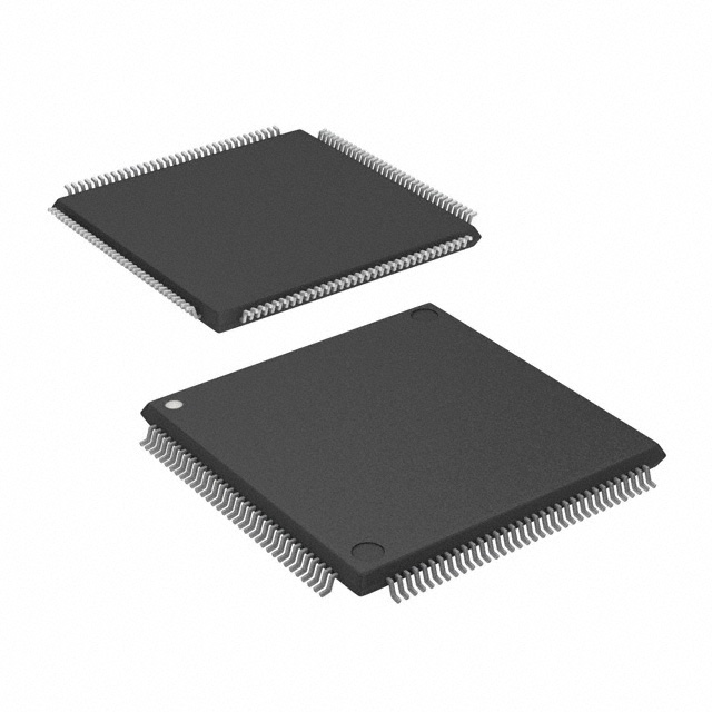
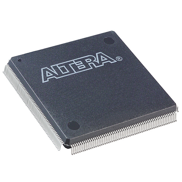
EP20K100ETC144-1N
| Part Description |
APEX-20KE® Field Programmable Gate Array (FPGA) IC 92 53248 4160 144-LQFP |
|---|---|
| Quantity | 57 Available (as of June 14, 2026) |

| Product Category | Field Programmable Gate Array (FPGA) |
|---|---|
| Manufacturer | Intel |
| Manufacturing Status | Obsolete |
| Manufacturer Standard Lead Time | Contact Us |
| Datasheet |
Specifications & Environmental
| Device Package | 144-TQFP (20x20) | Grade | Commercial | Operating Temperature | 0°C – 85°C | ||
|---|---|---|---|---|---|---|---|
| Package / Case | 144-LQFP | Number of I/O | 92 | Voltage | 1.71 V - 1.89 V | ||
| Mounting Method | Surface Mount | RoHS Compliance | Unknown | REACH Compliance | REACH Unaffected | ||
| Moisture Sensitivity Level | 3 (168 Hours) | Number of LABs/CLBs | 416 | Number of Logic Elements/Cells | 4160 | ||
| Number of Gates | 263000 | ECCN | 3A001A2A | HTS Code | 8542.39.0001 | ||
| Qualification | N/A | Total RAM Bits | 53248 |
Overview of EP20K100ETC144-1N – APEX-20KE® Field Programmable Gate Array (FPGA) IC 92 53248 4160 144-LQFP
The EP20K100ETC144-1N is an APEX-20KE family FPGA from Intel designed around a MultiCore architecture combining LUT-based logic, product-term logic and embedded memory blocks. It delivers a balanced mix of logic capacity, on-chip RAM and flexible I/O for embedded processing, memory-interface and I/O-intensive designs.
With 4,160 logic elements, approximately 53.2 kbits of embedded RAM, 92 user I/O pins and a 144-LQFP surface-mount package, this commercial-grade device targets applications that require moderate gate density with flexible clocking and interface capabilities.
Key Features
- Core architecture MultiCore architecture integrating LUT logic, product-term logic and embedded system blocks (ESBs) for a mix of register‑intensive and memory‑oriented functions.
- Logic capacity 4,160 logic elements and up to 263,000 system gates provide capacity for mid-range programmable logic tasks and glue‑logic implementations.
- Embedded memory Approximately 53,248 bits of on‑chip RAM (ESBs) suitable for FIFOs, dual‑port RAM and CAM-style functions.
- I/O and interfaces 92 user I/O pins with MultiVolt I/O support and programmable I/O features suitable for interfacing with a range of external peripherals and memory devices.
- Clocking and timing Family-level support for flexible clock management including multiple PLLs, a low‑skew clock tree and multiple global clock signals to support synchronous designs.
- Power and supply Internal and I/O supply support aligned with APEX‑20K family conventions; this device lists an operating voltage supply range of 1.71 V to 1.89 V.
- Package and mounting 144‑lead LQFP (surface mount); supplier device package listed as 144‑TQFP (20×20) for PCB footprint and assembly planning.
- Operating range and compliance Commercial temperature grade with an operating range of 0 °C to 85 °C and RoHS compliance for regulatory alignment.
Typical Applications
- Memory interface and buffering Use the device’s embedded RAM and ESB-based FIFOs for DDR/SDRAM buffering and ZBT-like memory controller logic.
- Peripheral and bus bridging Implement PCI/legacy bus bridging and peripheral glue logic leveraging flexible I/O levels and programmable I/O features.
- High‑speed serial and differential links Support LVDS and other differential signaling standards for channelized data paths and high‑throughput links.
- Embedded control and glue logic 4,160 logic elements and product‑term resources suit microcontroller offload, protocol handling and board‑level control functions.
Unique Advantages
- Balanced logic and memory mix: Combines 4,160 logic elements with about 53.2 kbits of embedded RAM to implement register‑heavy logic alongside on‑chip buffering and small memory structures.
- Flexible I/O capability: 92 user I/O pins with MultiVolt support enable direct interfacing to a range of external devices and memory types.
- Clock management features: Family-level PLLs and low‑skew clock tree features simplify implementation of multi‑clock designs and timing-critical logic.
- Commercial temperature qualification: Rated for 0 °C to 85 °C operation to meet standard commercial product requirements.
- Surface-mount packaging: 144‑lead LQFP package (144‑TQFP footprint reference) for compact PCB integration and automated assembly.
- RoHS compliant: Meets RoHS environmental requirements for reduced hazardous substances.
Why Choose EP20K100ETC144-1N?
The EP20K100ETC144-1N positions itself as a mid‑range APEX‑20KE FPGA option that balances logic density, embedded RAM and flexible I/O in a compact 144‑lead LQFP package. It is appropriate for designers who require a programmable logic device with solid on‑chip memory, multiple I/O voltage options and mature family features such as MultiCore architecture and advanced clock management.
Backed by the APEX‑20K family documentation and Intel’s manufacturing pedigree, this part offers a documented path for embedded logic, memory interface and bus‑bridge applications where commercial temperature operation and RoHS compliance are required.
Request a quote or submit a purchase inquiry to obtain pricing and availability for EP20K100ETC144-1N.


Date Founded: 1968
Headquarters: Santa Clara, California, USA
Employees: 130,000+
Revenue: $54.23 Billion
Certifications and Memberships: ISO9001:2015, ISO14001:2015, ISO17025:2017, ISO27001:2022, ISO45001:2018, ISO50001:2018


