
EP20K100ETC144-1X
| Part Description |
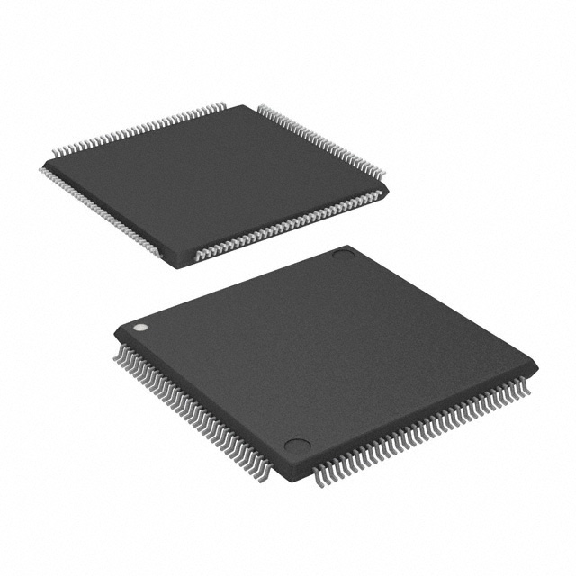
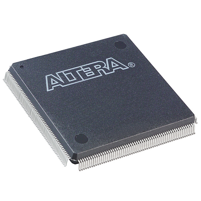
APEX-20KE® Field Programmable Gate Array (FPGA) IC 92 53248 4160 144-LQFP |
|---|---|
| Quantity | 693 Available (as of June 18, 2026) |

| Product Category | Field Programmable Gate Array (FPGA) |
|---|---|
| Manufacturer | Intel |
| Manufacturing Status | Obsolete |
| Manufacturer Standard Lead Time | Contact Us |
| Datasheet |
Specifications & Environmental
| Device Package | 144-TQFP (20x20) | Grade | Commercial | Operating Temperature | 0°C – 85°C | ||
|---|---|---|---|---|---|---|---|
| Package / Case | 144-LQFP | Number of I/O | 92 | Voltage | 1.71 V - 1.89 V | ||
| Mounting Method | Surface Mount | RoHS Compliance | Unknown | REACH Compliance | REACH Unaffected | ||
| Moisture Sensitivity Level | 3 (168 Hours) | Number of LABs/CLBs | 416 | Number of Logic Elements/Cells | 4160 | ||
| Number of Gates | 263000 | ECCN | 3A001A2A | HTS Code | 8542.39.0001 | ||
| Qualification | N/A | Total RAM Bits | 53248 |
Overview of EP20K100ETC144-1X – APEX-20KE® Field Programmable Gate Array (FPGA) IC 92 53248 4160 144-LQFP
The EP20K100ETC144-1X is an APEX-20KE family FPGA in a 144-LQFP surface-mount package, providing programmable logic, embedded memory, and flexible I/O in a commercial-grade device. Its MultiCore architecture integrates LUT-based logic, product-term logic and embedded system blocks (ESBs) to support both register‑intensive and memory‑centric functions.
With 4,160 logic elements, approximately 53,248 bits of on-chip RAM, 92 user I/O pins and a maximum of 263,000 system gates, this device targets designs that require mid-density programmable logic, on-chip memory for FIFOs or dual-port RAM, and configurable high-performance I/O. The device operates from a 1.71 V to 1.89 V supply and supports an ambient temperature range of 0 °C to 85 °C.
Key Features
- Core architecture MultiCore architecture combining LUT logic, product-term logic and embedded system blocks (ESBs) for register‑intensive and memory‑oriented functions.
- Logic capacity 4,160 logic elements (LEs) and up to 263,000 system gates provide mid-range programmable logic resources for custom digital functions.
- Embedded memory Approximately 53,248 bits of on-chip RAM suitable for FIFOs, dual-port RAM and small data buffers implemented in ESBs.
- I/O and interface support 92 user I/O pins with family-level support for MultiVolt I/O, advanced I/O standards and high-speed memory interfaces; programmable output slew-rate and individual tri-state control help manage signal integrity.
- Clock management Flexible clock resources including up to four PLLs, a built-in low-skew clock tree and features for phase/ delay control, enabling deterministic system timing.
- Power and low-power options Designed for low-power operation with an ESB programmable power-saving mode and a defined supply range of 1.71 V to 1.89 V.
- Package and operating range Surface-mount 144-LQFP (144-TQFP 20×20 footprint) package; commercial-grade device rated for 0 °C to 85 °C operation.
Typical Applications
- System integration and SOPC designs Use embedded system blocks and LUT logic to implement on-chip FIFOs, dual-port RAM and content-addressable memory for compact system-on-programmable-chip implementations.
- High-speed memory interfaces Deploy the device where support for external high-speed memories such as DDR SDRAM is required alongside programmable logic for control and buffering.
- PCI and peripheral bridging Leverage the family-level support for PCI Local Bus signaling and high-performance I/O to implement bus interfaces and protocol bridging.
- Custom control and data-path logic Implement register-intensive and combinatorial functions using LUT logic and product-term resources for application-specific processing and control tasks.
Unique Advantages
- Highly integrated architecture: Combines LUT logic, product-term logic and ESBs to reduce external component count and simplify board-level design.
- Balanced logic and memory: 4,160 logic elements paired with ~53,248 bits of embedded RAM allow simultaneous implementation of control logic and local data storage.
- Flexible, high-performance I/O: 92 I/O pins with MultiVolt support and programmable I/O controls enable direct interfacing with a variety of external devices and memory types.
- Deterministic clocking: Up to four PLLs and a low-skew clock distribution support reliable timing for synchronous designs and high-speed interfaces.
- Commercial-grade, surface-mount package: 144-LQFP surface-mount package and 0 °C to 85 °C operating range suit a wide array of commercial embedded applications.
Why Choose EP20K100ETC144-1X?
The EP20K100ETC144-1X offers a practical balance of programmable logic, embedded memory and flexible I/O in a compact 144-LQFP package. Its MultiCore architecture and ESB capabilities make it well suited for designs that require both register‑intensive logic and on-chip memory resources, while clock management and I/O flexibility support reliable interfacing with high-speed peripherals and external memories.
Engineers seeking a commercial‑grade, mid-density FPGA for system integration, protocol bridging or custom data-path control will find this device provides verifiable, on-chip resources and configurable power/clock options to simplify board design and accelerate development.
Request a quote or submit a pricing inquiry today to evaluate EP20K100ETC144-1X for your next programmable-logic design.


Date Founded: 1968
Headquarters: Santa Clara, California, USA
Employees: 130,000+
Revenue: $54.23 Billion
Certifications and Memberships: ISO9001:2015, ISO14001:2015, ISO17025:2017, ISO27001:2022, ISO45001:2018, ISO50001:2018


