
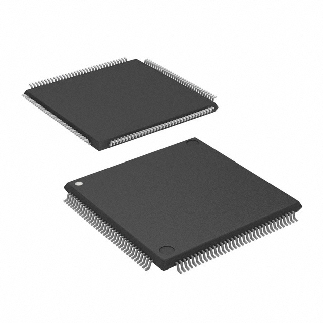
EP20K100ETC144-3
| Part Description |
APEX-20KE® Field Programmable Gate Array (FPGA) IC 92 53248 4160 144-LQFP |
|---|---|
| Quantity | 1,812 Available (as of June 15, 2026) |

| Product Category | Field Programmable Gate Array (FPGA) |
|---|---|
| Manufacturer | Intel |
| Manufacturing Status | Obsolete |
| Manufacturer Standard Lead Time | Contact Us |
| Datasheet |
Specifications & Environmental
| Device Package | 144-TQFP (20x20) | Grade | Commercial | Operating Temperature | 0°C – 85°C | ||
|---|---|---|---|---|---|---|---|
| Package / Case | 144-LQFP | Number of I/O | 92 | Voltage | 1.71 V - 1.89 V | ||
| Mounting Method | Surface Mount | RoHS Compliance | Unknown | REACH Compliance | REACH Unaffected | ||
| Moisture Sensitivity Level | 3 (168 Hours) | Number of LABs/CLBs | 416 | Number of Logic Elements/Cells | 4160 | ||
| Number of Gates | 263000 | ECCN | 3A001A2A | HTS Code | 8542.39.0001 | ||
| Qualification | N/A | Total RAM Bits | 53248 |
Overview of EP20K100ETC144-3 – APEX-20KE FPGA, 4,160 Logic Elements, 92 I/O, 144‑LQFP
The EP20K100ETC144-3 is an APEX‑20KE family field programmable gate array (FPGA) supplied in a 144‑lead LQFP package. It implements the APEX MultiCore architecture combining look‑up table (LUT) logic, product‑term logic, and embedded memory blocks to support register‑intensive and memory‑intensive functions.
With 4,160 logic elements, 53,248 bits of on‑chip RAM, and 92 user I/O pins, this device is suited for designs that require embedded memory functions (FIFOs, dual‑port RAM, CAM), flexible I/O interfacing, and integrated clock management while operating within a commercial temperature range.
Key Features
- Core Architecture APEX MultiCore architecture integrating LUT logic and product‑term logic for register‑ and combinatorial‑intensive functions; approximately 263,000 system gates.
- Logic Density 4,160 logic elements (LEs) to implement custom digital logic and state machines.
- Embedded Memory 53,248 total RAM bits of on‑chip memory for FIFOs, dual‑port RAM, and content‑addressable memory (CAM) implementations.
- I/O and Interface 92 user I/O pins with advanced I/O capabilities described in the APEX 20K family, including MultiVolt I/O interface support and high‑speed interface options.
- Clock Management Family features include flexible clock management with multiple PLLs, a low‑skew clock tree, and programmable clock phase/delay controls for synchronized system timing.
- Power Device supply operation specified at 1.71 V to 1.89 V; family features include programmable power‑saving modes for embedded system blocks.
- Package and Mounting Supplied in a 144‑LQFP package (supplier device package 144‑TQFP, 20×20) for surface‑mount PCB designs.
- Operating Range and Compliance Commercial grade operation from 0 °C to 85 °C; RoHS compliant.
Typical Applications
- Embedded system integration Implement SOPC‑style functionality where on‑chip LUT logic and embedded memory are used to consolidate system functions and reduce external components.
- Memory buffering and FIFO control Use the on‑chip RAM and ESB capabilities to implement high‑efficiency FIFOs and dual‑port RAM for data staging and flow control.
- High‑speed interface bridging Deploy the device for protocol bridging and interface logic that benefits from flexible I/O and clock management features.
- Custom logic and control Implement finite state machines, control logic, and combinatorial‑intensive functions using the device’s LUT and product‑term resources.
Unique Advantages
- Integrated memory and logic: Combines LUT‑based logic with embedded system blocks to implement memory‑centric functions without extensive external RAM.
- Flexible clocking: Built‑in PLLs and programmable clock features simplify timing distribution and reduce external clocking complexity.
- Compact package with robust I/O count: 92 user I/Os in a 144‑LQFP package enable dense connectivity in space‑constrained board designs.
- Commercial temperature suitability: Rated for 0 °C to 85 °C, appropriate for a wide range of commercial and industrial control applications.
- Standards‑oriented I/O capabilities: Family features include MultiVolt I/O support and signals suitable for common high‑speed memory and interface use cases.
Why Choose EP20K100ETC144-3?
The EP20K100ETC144-3 offers a balanced mix of logic density, embedded memory, and flexible I/O in a compact 144‑LQFP package. Its APEX MultiCore architectural approach lets designers consolidate register‑heavy and memory‑heavy functions on a single device, reducing board complexity and BOM count.
This FPGA is appropriate for teams developing embedded systems, interface logic, or buffer/FIFO functions that require on‑chip RAM and configurable clocking. The combination of 4,160 logic elements, 53,248 bits of embedded memory, and dedicated I/O resources makes it a practical choice for mid‑density programmable logic requirements where commercial temperature range and RoHS compliance are required.
Request a quote or submit an availability inquiry for EP20K100ETC144-3 to receive pricing and lead‑time information tailored to your project needs.


Date Founded: 1968
Headquarters: Santa Clara, California, USA
Employees: 130,000+
Revenue: $54.23 Billion
Certifications and Memberships: ISO9001:2015, ISO14001:2015, ISO17025:2017, ISO27001:2022, ISO45001:2018, ISO50001:2018


