
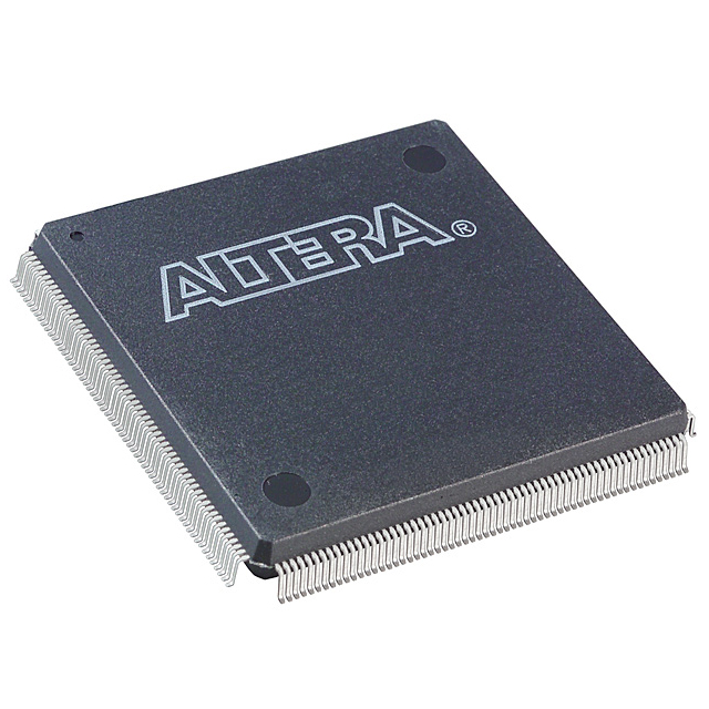
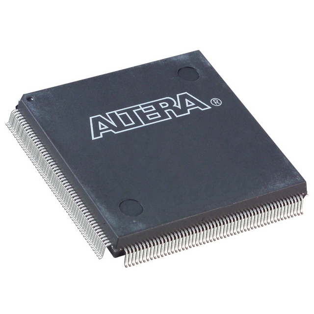
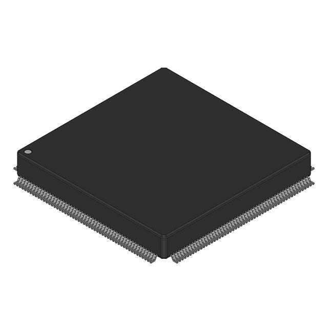
EP20K100QC240-3
| Part Description |
APEX-20K® Field Programmable Gate Array (FPGA) IC 189 53248 4160 240-BFQFP |
|---|---|
| Quantity | 1,243 Available (as of June 15, 2026) |

| Product Category | Field Programmable Gate Array (FPGA) |
|---|---|
| Manufacturer | Intel |
| Manufacturing Status | Obsolete |
| Manufacturer Standard Lead Time | Contact Us |
| Datasheet |
Specifications & Environmental
| Device Package | 240-PQFP (32x32) | Grade | Commercial | Operating Temperature | 0°C – 85°C | ||
|---|---|---|---|---|---|---|---|
| Package / Case | 240-BFQFP | Number of I/O | 189 | Voltage | 2.375 V - 2.625 V | ||
| Mounting Method | Surface Mount | RoHS Compliance | RoHS non-compliant | REACH Compliance | REACH Unaffected | ||
| Moisture Sensitivity Level | 3 (168 Hours) | Number of LABs/CLBs | 416 | Number of Logic Elements/Cells | 4160 | ||
| Number of Gates | 263000 | ECCN | 3A991D | HTS Code | 8542.39.0001 | ||
| Qualification | N/A | Total RAM Bits | 53248 |
Overview of EP20K100QC240-3 – APEX-20K® Field Programmable Gate Array (FPGA) IC 189 53248 4160 240-BFQFP
The EP20K100QC240-3 is a field programmable gate array (FPGA) in Intel’s APEX-20K family, implementing a MultiCore architecture that integrates look-up table (LUT) logic, product-term logic, and embedded memory blocks. This commercial-grade, surface-mount device combines on-chip logic, embedded RAM, and flexible I/O to address programmable-logic designs that require moderate gate density, embedded data buffering, and configurable I/O.
Key attributes include 4,160 logic elements, approximately 53 kbits of embedded memory, 189 I/O pins, and a 240-pin BFQFP package, making the device suitable for compact, board-level FPGA implementations in commercial electronic products.
Key Features
- APEX-20K MultiCore Architecture Integrates LUT-based logic, product-term logic and embedded system blocks (ESBs) for implementing memory functions such as FIFOs, dual-port RAM, and CAM.
- Logic Capacity Provides 4,160 logic elements and a device gate count listed as 263,000, enabling moderate-density programmable logic implementations.
- Embedded Memory Approximately 53,248 bits of on-chip RAM available for data buffering and small on-chip storage needs.
- I/O and Interface Flexibility 189 user I/O pins with MultiVolt I/O interface support per the APEX-20K family, enabling interfacing with a range of external signaling levels.
- Clock Management Family-level clock features include up to four PLLs, a low-skew clock tree, support for up to eight global clocks, and programmable phase/delay control (ClockLock, ClockBoost, ClockShift).
- High-speed Memory & Bus Support Family documentation notes support for high-speed external memories (including DDR SDRAM and ZBT SRAM) and compliance with PCI Local Bus Specification for 3.3-V operation at 33/66 MHz (per APEX-20K family guidance).
- Package & Mounting Surface-mount 240-BFQFP package (supplier device package: 240-PQFP 32×32) for compact board layouts.
- Power & Temperature Internal supply range specified at 2.375 V to 2.625 V and commercial operating temperature of 0 °C to 85 °C; the family is designed with low-power operation and programmable power-saving modes.
- Compliance RoHS compliant.
Typical Applications
- Memory Interface and Buffering Implement DDR SDRAM or ZBT SRAM interfaces and on-chip FIFOs using embedded system blocks for data buffering and memory control functions.
- High-speed I/O and Protocol Bridging Use the device’s MultiVolt I/O and family-level support for LVDS and PCI signaling to implement protocol bridging, bus interface logic, or front-end I/O processing.
- Embedded System Integration (SOPC) Leverage the APEX-20K MultiCore architecture for system-on-a-programmable-chip designs that combine logic, memory, and I/O in a single device.
- Custom Logic and Prototyping Deploy as a compact, surface-mount FPGA for board-level prototyping and custom digital logic functions in commercial electronic products.
Unique Advantages
- Highly integrated MultiCore design: Combines LUT logic, product-term logic and ESBs to reduce external component count for memory and control functions.
- Balanced logic and memory resources: 4,160 logic elements paired with approximately 53 kbits of embedded RAM supports register-intensive logic and on-chip buffering without sacrificing logic capacity.
- Flexible I/O and interface support: 189 I/O pins and family-level MultiVolt I/O capability enable interfacing with multiple signaling standards and external devices.
- Deterministic clocking and PLLs: Up to four PLLs and a low-skew clock tree simplify clock distribution for synchronous designs and multi-clock domains.
- Compact surface-mount package: 240-BFQFP (240-PQFP 32×32) offers a board-friendly pinout for space-constrained applications.
- Commercial-grade and RoHS compliant: Designed for commercial temperature ranges (0 °C to 85 °C) and meets RoHS environmental requirements.
Why Choose EP20K100QC240-3?
The EP20K100QC240-3 brings APEX-20K family capabilities—integrated LUT and product-term logic, embedded system blocks, and flexible clock and I/O features—into a compact 240-pin BFQFP package. Its combination of 4,160 logic elements, on-chip RAM, and 189 I/O pins makes it appropriate for commercial designs that need embedded memory, configurable I/O, and deterministic clocking without a large footprint.
This device is suited to engineers and teams implementing board-level programmable logic, memory interfaces, and I/O-rich control functions who require a commercially graded, RoHS-compliant FPGA backed by the APEX-20K family documentation and feature set.
Request a quote or submit an inquiry to obtain pricing and availability for the EP20K100QC240-3 and accelerate evaluation for your next design.


Date Founded: 1968
Headquarters: Santa Clara, California, USA
Employees: 130,000+
Revenue: $54.23 Billion
Certifications and Memberships: ISO9001:2015, ISO14001:2015, ISO17025:2017, ISO27001:2022, ISO45001:2018, ISO50001:2018


