
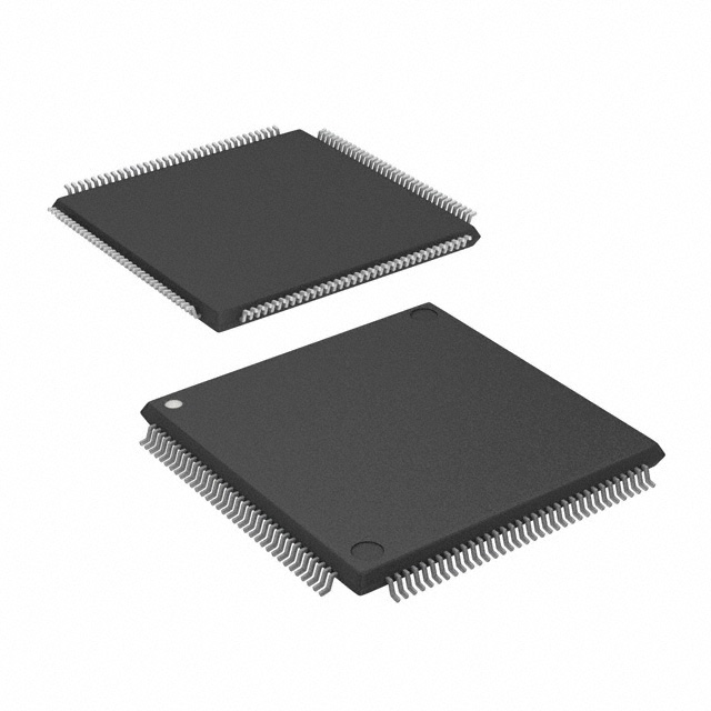
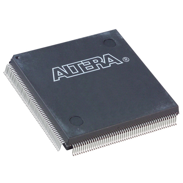
EP2C5T144C6N
| Part Description |
Cyclone® II Field Programmable Gate Array (FPGA) IC 89 119808 4608 144-LQFP |
|---|---|
| Quantity | 377 Available (as of June 10, 2026) |

| Product Category | Field Programmable Gate Array (FPGA) |
|---|---|
| Manufacturer | Intel |
| Manufacturing Status | Active |
| Manufacturer Standard Lead Time | 26 Weeks |
| Datasheet |
Specifications & Environmental
| Device Package | 144-TQFP (20x20) | Grade | Commercial | Operating Temperature | 0°C – 85°C | ||
|---|---|---|---|---|---|---|---|
| Package / Case | 144-LQFP | Number of I/O | 89 | Voltage | 1.15 V - 1.25 V | ||
| Mounting Method | Surface Mount | RoHS Compliance | RoHS Compliant | REACH Compliance | REACH Unaffected | ||
| Moisture Sensitivity Level | 3 (168 Hours) | Number of LABs/CLBs | 288 | Number of Logic Elements/Cells | 4608 | ||
| Number of Gates | N/A | ECCN | 3A991D | HTS Code | 8542.39.0001 | ||
| Qualification | N/A | Total RAM Bits | 119808 |
Overview of EP2C5T144C6N – Cyclone® II FPGA, 4,608 Logic Elements, 144-LQFP
The EP2C5T144C6N is a Cyclone® II Field Programmable Gate Array (FPGA) from Intel, provided in a 144-pin LQFP surface-mount package. It implements approximately 4,608 logic elements and integrates on-chip resources tailored for low-cost embedded processing and DSP-oriented designs.
Designed for commercial-grade applications, this device combines a compact 144-LQFP footprint, multi-volt I/O capabilities and the Cyclone II family architecture features such as dedicated clock networks and programmable I/O to support interface bridging, embedded control and DSP tasks.
Key Features
- Logic Capacity Approximately 4,608 logic elements to implement custom digital logic, control paths and glue logic within a compact FPGA footprint.
- Embedded Memory Approximately 119,808 bits of embedded memory (~0.12 Mbits) for FIFOs, buffering and small on-chip data stores.
- I/O Resources 89 general I/O pins with the Cyclone II I/O structure and advanced I/O standard support for flexible interfacing to external devices.
- Clocking and Timing Family-level features include a global clock network and phase-locked loops (PLLs) to support synchronized multi-clock designs.
- DSP Support Cyclone II family includes embedded multipliers and DSP-oriented resources useful for arithmetic- and signal-processing tasks.
- Configuration & Test IEEE Std. 1149.1 (JTAG) boundary-scan support and multiple configuration options as described in the Cyclone II device documentation.
- Power Core supply range from 1.15 V to 1.25 V to match system power domains and enable predictable power budgeting.
- Package & Mounting 144-LQFP (supplier device package listed as 144-TQFP 20×20) surface-mount package suitable for dense PCB layouts.
- Operating Range & Compliance Commercial-grade operating temperature of 0 °C to 85 °C and RoHS compliant.
Typical Applications
- Low‑Cost Embedded Processing Implement control logic, state machines and embedded processing tasks where a small, cost-effective FPGA is required.
- Low‑Cost DSP Solutions Use embedded multipliers and on-chip memory for basic DSP functions such as filtering, decimation and simple signal processing pipelines.
- Interface Bridging & Protocol Conversion Leverage the programmable I/O and clocking resources to connect and translate between different standards and external peripherals.
- Prototyping & Evaluation Compact package and accessible I/O count make the device suitable for board-level prototyping and early system validation.
Unique Advantages
- Balanced Logic and Memory Combines ~4,608 logic elements with ~119,808 bits of embedded memory, enabling integration of control, buffering and modest data-processing functions on a single device.
- Flexible I/O and Clocking 89 I/O pins plus family-level support for advanced I/O standards and a global clock/PLL architecture simplify timing and interface design.
- Compact Surface-Mount Package 144-LQFP (20×20 TQFP format) offers a small board footprint for space-constrained designs while maintaining adequate I/O.
- Commercial-Grade Reliability Rated for 0 °C to 85 °C operation and RoHS compliant, suitable for mainstream commercial and consumer electronics applications.
- Established Family Features Built on the Cyclone II architecture with supported features such as embedded multipliers, configurable memory modes and JTAG boundary-scan for testability and flexible implementation.
Why Choose EP2C5T144C6N?
The EP2C5T144C6N positions itself as a compact, cost-conscious Cyclone II FPGA solution that brings together a useful balance of logic capacity, on-chip memory and flexible I/O in a commercial-grade LQFP package. Its supported family features—clocking resources, embedded multipliers, and JTAG—help streamline implementation of embedded control, interface bridging and basic DSP functions.
This device is well suited for engineers and procurement teams designing small to medium-complexity digital systems that require an integrated programmable logic solution with predictable supply, package and temperature characteristics backed by the Cyclone II device documentation.
Request a quote or submit a quote request today to get pricing and availability for EP2C5T144C6N and to discuss quantity and delivery options.


Date Founded: 1968
Headquarters: Santa Clara, California, USA
Employees: 130,000+
Revenue: $54.23 Billion
Certifications and Memberships: ISO9001:2015, ISO14001:2015, ISO17025:2017, ISO27001:2022, ISO45001:2018, ISO50001:2018


