
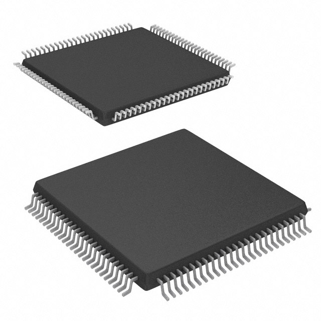
M1A3P250-2FGG144
| Part Description |
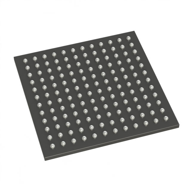
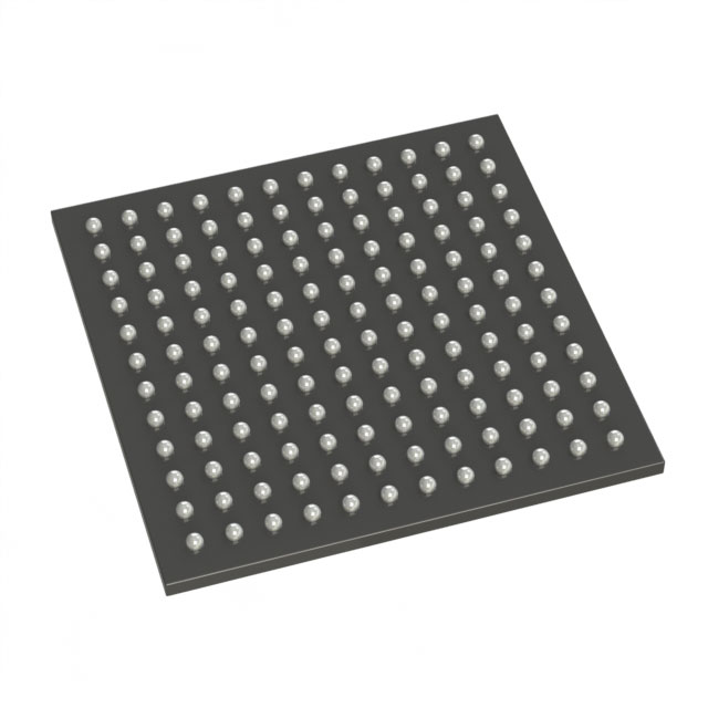
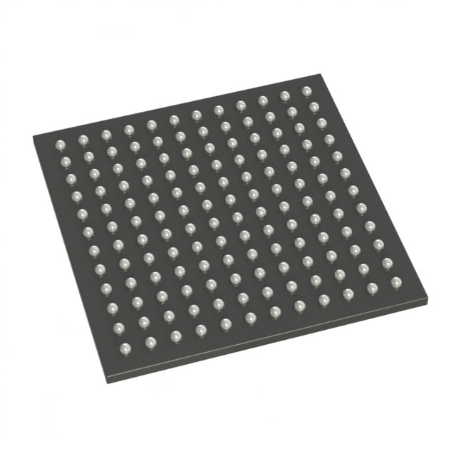
ProASIC3 Field Programmable Gate Array (FPGA) IC 97 36864 144-LBGA |
|---|---|
| Quantity | 1,915 Available (as of October 8, 2026) |
| Product Category | Field Programmable Gate Array (FPGA) |
|---|---|
| Manufacturer | Microchip Technology |
| Manufacturing Status | Active |
| Manufacturer Standard Lead Time | 18 Weeks |
| Datasheet |
Specifications & Environmental
| Device Package | 144-FPBGA (13x13) | Grade | Commercial | Operating Temperature | 0°C – 85°C | ||
|---|---|---|---|---|---|---|---|
| Package / Case | 144-LBGA | Number of I/O | 97 | Voltage | 1.425 V - 1.575 V | ||
| Mounting Method | Surface Mount | RoHS Compliance | ROHS3 Compliant | REACH Compliance | REACH Unaffected | ||
| Moisture Sensitivity Level | 3 (168 Hours) | Number of LABs/CLBs | 6144 | Number of Logic Elements/Cells | 6144 | ||
| Number of Gates | 250000 | ECCN | 3A991D | HTS Code | 8542.39.0001 | ||
| Qualification | N/A | Total RAM Bits | 36864 |
Overview of M1A3P250-2FGG144 – ProASIC3 FPGA, 97 I/O, 36,864-bit RAM, 144-LBGA
The M1A3P250-2FGG144 is a ProASIC3 field programmable gate array (FPGA) IC from Microchip Technology designed for commercial embedded applications. It integrates a mid-range logic capacity with on-chip RAM and a 97-pin I/O complement in a compact 144-LBGA package to support custom digital logic, interface bridging, and control functions.
With 6,144 logic elements, approximately 36,864 bits of embedded memory, and a 1.425 V–1.575 V supply window, this device targets designs that require moderate programmable logic density in surface-mount board assemblies operating in commercial temperature environments.
Key Features
- Logic Capacity — 6,144 logic elements (cells) providing a programmable fabric suitable for glue logic, state machines, and custom datapaths; rated at 250,000 equivalent gates.
- Embedded Memory — 36,864 bits of on-chip RAM (approximately 0.037 Mbits) to support buffering, FIFOs, and small lookup tables without external memory.
- I/O Count — 97 I/O pins to accommodate multiple peripheral interfaces and board-level signals.
- Power Supply — Operates from a 1.425 V to 1.575 V supply range for integration into standardized power rails.
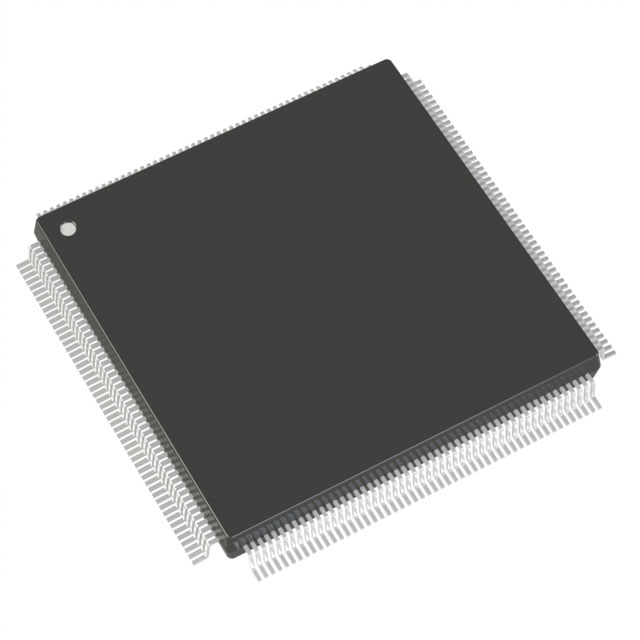
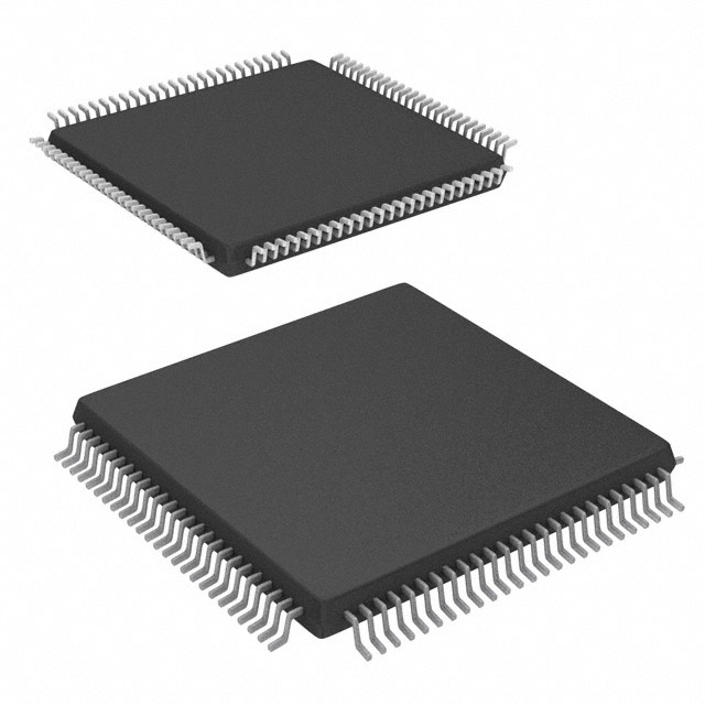
- Package and Mounting — 144-LBGA package (supplier package: 144-FPBGA, 13×13) designed for surface-mount assembly to save PCB area and enable high-density layouts.
- Operating Range — Commercial grade operation from 0°C to 85°C for a wide range of consumer and light industrial environments.
- Environmental Compliance — RoHS compliant, supporting regulatory requirements for lead-free assemblies.
Typical Applications
- Embedded Control — Implement custom control logic, state machines, and interface sequencing for commercial embedded products.
- Protocol Bridging — Provide flexible I/O and programmable logic to adapt or translate between digital interfaces on a single board.
- Prototyping and Development — Use as a programmable platform for validating digital designs and iterating firmware-hardware interactions.
Unique Advantages
- Balanced Logic and Memory — 6,144 logic elements combined with on-chip RAM enables compact implementations of control and buffering functions without external components.
- Generous I/O Count — 97 I/O pins allow integration of multiple peripherals and signal domains on a single FPGA device.
- Compact Surface-Mount Package — 144-LBGA (144-FPBGA, 13×13) minimizes PCB footprint while supporting high-density board designs.
- Commercial Temperature Rating — Rated for 0°C to 85°C environments, suitable for consumer and general-purpose commercial applications.
- Regulatory Compatibility — RoHS compliant to simplify assembly and materials planning for lead-free manufacturing.
Why Choose M1A3P250-2FGG144?
The M1A3P250-2FGG144 offers a practical combination of logic density, embedded memory, and I/O capacity in a compact 144-LBGA package, making it a solid choice for commercial embedded designs that need programmable logic without excessive board space or external memory. Its supply voltage range and commercial temperature rating align with common system power rails and deployment conditions.
Designed and manufactured by Microchip Technology, this ProASIC3 FPGA provides a predictable platform for customers building moderate-complexity digital systems, enabling consolidation of glue logic, interface adaptation, and custom control functions into a single surface-mount device.
Request a quote or submit an inquiry to obtain pricing and availability for the M1A3P250-2FGG144 and integrate this ProASIC3 FPGA into your next commercial embedded design.





















Date Founded: 1989
Headquarters: Chandler, Arizona, USA
Employees: 22,000+
Revenue: $8.349 Billion
Certifications and Memberships: ISO9001:2015, IATF16949:2016, AS 9100D




