
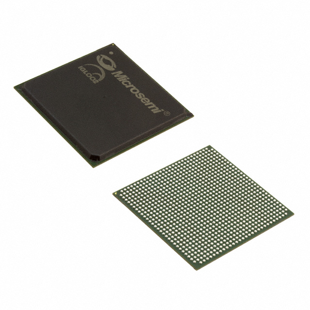
M2GL050-1FG896
| Part Description |
IGLOO2 Field Programmable Gate Array (FPGA) IC 377 1869824 56340 896-BGA |
|---|---|
| Quantity | 895 Available (as of June 15, 2026) |
| Product Category | Field Programmable Gate Array (FPGA) |
|---|---|
| Manufacturer | Microchip Technology |
| Manufacturing Status | Active |
| Manufacturer Standard Lead Time | 16 Weeks |
| Datasheet |
Specifications & Environmental
| Device Package | 896-FBGA (31x31) | Grade | Commercial | Operating Temperature | 0°C – 85°C | ||
|---|---|---|---|---|---|---|---|
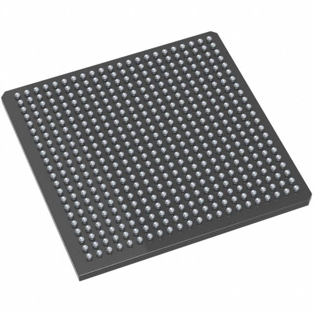
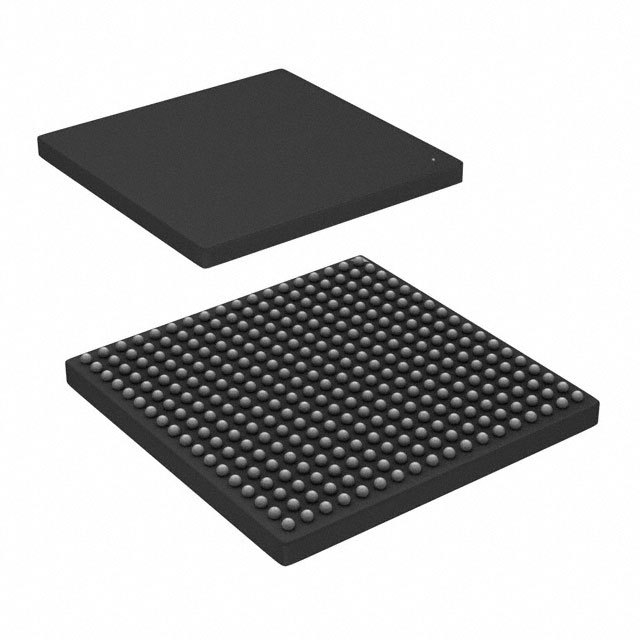
| Package / Case | 896-BGA | Number of I/O | 377 | Voltage | 1.14 V - 2.625 V | ||
| Mounting Method | Surface Mount | RoHS Compliance | RoHS non-compliant | REACH Compliance | REACH Unaffected | ||
| Moisture Sensitivity Level | 3 (168 Hours) | Number of LABs/CLBs | 56340 | Number of Logic Elements/Cells | 56340 | ||
| Number of Gates | N/A | ECCN | 3A991D | HTS Code | 8542.39.0001 | ||
| Qualification | N/A | Total RAM Bits | 1869824 |
Overview of M2GL050-1FG896 – IGLOO2 Field Programmable Gate Array (FPGA) IC 377 1869824 56340 896-BGA
The M2GL050-1FG896 is an IGLOO2 flash-based FPGA optimized for low-power, secure and high-performance programmable logic applications. Built on the IGLOO2 architecture, it combines a substantial logic fabric with multi-standard I/Os and integrated memory to address communication, signal processing and embedded control use cases.
With 56,340 logic elements, 377 user I/Os, and an 896-ball FBGA (31 × 31) package, this commercial-grade device targets designs that require dense logic, flexible I/O, and a broad supply voltage range for diverse board-level integrations.
Key Features
- Logic Capacity — 56,340 logic elements provide a large programmable fabric suitable for complex glue-logic, protocol handling, and moderate DSP tasks.
- Embedded Memory — Approximately 1.87 Mbits of on-chip RAM (1,869,824 total RAM bits) for LUTs, FIFOs and buffering requirements; the IGLOO2 family also offers embedded SRAM and nonvolatile memory options at the subsystem level.
- High I/O Count — 377 user I/Os support multi-standard signaling and flexible board-level interfacing in a single device.
- Package and Mounting — 896-FBGA (31 × 31) surface-mount package suitable for compact, high-density PCB layouts.
- Supply Voltage Range — Operates across 1.14 V to 2.625 V to accommodate a variety of core and I/O domain configurations.
- Operating Temperature — Commercial-grade specification from 0 °C to 85 °C for general embedded and consumer applications.
- Family-Level High-Speed Interfaces — IGLOO2 family features include support for up to 16 SERDES lanes, PCIe endpoint cores (x1/x2/x4), and high-speed memory controllers (up to 2 DDRx controllers) for designs requiring serial links and external DDR memory interfaces.
- DSP and Math — IGLOO2 architecture provides dedicated mathblocks for DSP operations (family-level capability up to 240 fast mathblocks), enabling efficient multiply-accumulate and signal-processing implementations.
- Clocking and PLLs — Family clock resources include multiple oscillators and up to eight clock conditioning circuits with integrated PLLs for flexible clock generation and distribution.
- Security and Reliability — IGLOO2 family security features include encrypted bitstream loading, supply-chain assurance device certificates, anti-tamper protections and zeroization options to help protect IP and sensitive designs.
- Compliance — RoHS compliant for environmentally conscious manufacturing and assembly.
Typical Applications
- High-speed Communications — Implement protocol bridging, serialization/deserialization and PHY interfacing using the IGLOO2 family’s SERDES and PCIe capabilities.
- Memory Interface and Buffering — Use the on-chip RAM alongside DDRx controller support to build memory controllers, data buffering and packet reordering functions.
- DSP and Signal Processing — Leverage embedded mathblocks and ample logic elements for filtering, FFTs, and real-time signal conditioning tasks.
- Secure Embedded Systems — Deploy encrypted bitstreams and hardware security features to protect IP and enable secure boot or secure configuration workflows.
Unique Advantages
- High Logic Density: 56,340 logic elements allow consolidation of multiple functions into a single FPGA, reducing board-level component count.
- Broad I/O Flexibility: 377 user I/Os enable mixed-signal and mixed-standard interfacing without external translators, simplifying system routing.
- Integrated Memory Resources: Nearly 1.87 Mbits of on-chip RAM combined with family-level eSRAM/eNVM options provide versatile storage for buffers, state machines and configuration data.
- Scalable Performance Options: Family support for SERDES lanes, PCIe and DDRx controllers lets designers scale bandwidth and external memory performance as system needs evolve.
- Security-Ready: Built-in device and bitstream protection features support supply-chain assurance and encrypted configuration for IP-sensitive designs.
- Commercial Temperature Range: Rated 0 °C to 85 °C for reliable operation across typical embedded and consumer operating environments.
Why Choose M2GL050-1FG896?
The M2GL050-1FG896 combines a substantial logic fabric with a high I/O count and integrated memory to deliver a flexible platform for communications, embedded control and signal-processing applications. Its IGLOO2 architecture brings family-level features—such as low-power flash-based configuration, security options and high-speed interface support—that align with designs requiring a balance of performance, integration and on-board security.
This device is well suited to engineers and procurement teams looking for a commercially graded FPGA in an 896-FBGA package that supports a wide voltage range and robust on-chip resources, enabling compact, reliable system designs with scalable peripheral and memory interfaces.
Request a quote or submit a pricing and availability inquiry to receive lead-time and procurement details for the M2GL050-1FG896.


Date Founded: 1989
Headquarters: Chandler, Arizona, USA
Employees: 22,000+
Revenue: $8.349 Billion
Certifications and Memberships: ISO9001:2015, IATF16949:2016, AS 9100D


