
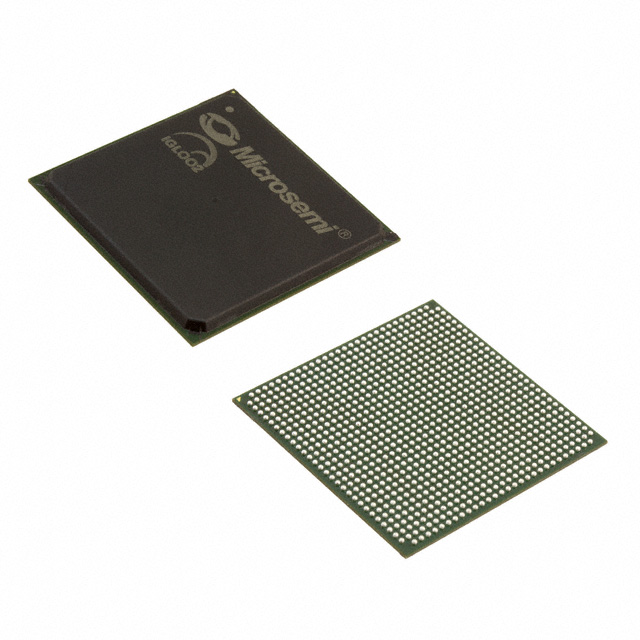
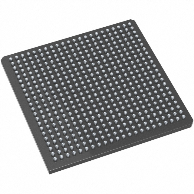
M2GL050-1FGG484I
| Part Description |
IGLOO2 Field Programmable Gate Array (FPGA) IC 267 1869824 56340 484-BGA |
|---|---|
| Quantity | 379 Available (as of June 10, 2026) |

| Product Category | Field Programmable Gate Array (FPGA) |
|---|---|
| Manufacturer | Microchip Technology |
| Manufacturing Status | Active |
| Manufacturer Standard Lead Time | 16 Weeks |
| Datasheet |
Specifications & Environmental
| Device Package | 484-FPBGA (23x23) | Grade | Industrial | Operating Temperature | -40°C – 100°C | ||
|---|---|---|---|---|---|---|---|
| Package / Case | 484-BGA | Number of I/O | 267 | Voltage | 1.14 V - 2.625 V | ||
| Mounting Method | Surface Mount | RoHS Compliance | ROHS3 Compliant | REACH Compliance | REACH Unaffected | ||
| Moisture Sensitivity Level | 3 (168 Hours) | Number of LABs/CLBs | 56340 | Number of Logic Elements/Cells | 56340 | ||
| Number of Gates | N/A | ECCN | 3A991D | HTS Code | 8542.39.0001 | ||
| Qualification | N/A | Total RAM Bits | 1869824 |
Overview of M2GL050-1FGG484I – IGLOO2 FPGA, 56,340 Logic Elements, 267 I/Os, 484-BGA
The M2GL050-1FGG484I is an IGLOO2 flash-based Field Programmable Gate Array (FPGA) from Microchip Technology, offered in a 484-ball BGA package. It combines 56,340 logic elements with on-chip memory and a broad I/O set to address embedded processing, high-speed communication interfaces, and secure/low-power designs.
Targeted at industrial applications, this device provides a balance of integration, non-volatile configuration, and operational range—supporting designs that require substantial logic capacity, multi-standard I/O, and industrial temperature operation.
Key Features
- Core Logic 56,340 logic elements provide a sizeable programmable fabric for control, processing, and glue-logic implementations.
- Embedded Memory Approximately 1.87 Mbits of on-chip RAM (1,869,824 bits) to support buffering, state storage, and local data paths.
- I/O Capacity & Voltage 267 user I/Os with a supply range of 1.14 V to 2.625 V to support multiple signaling standards and flexible power domains.
- Family-Level Interfaces IGLOO2 family capabilities include high-speed serial interfaces (PCIe, XAUI/XGXS), native SERDES, and DDR2/DDR3 memory controller support—enabling high-bandwidth communication and memory interfacing in system designs.
- DSP and Math Resources IGLOO2 architecture includes mathblocks for DSP operations (documented at the family level) to accelerate signed/unsigned multiplication and accumulation tasks.
- Non-Volatile, Flash-Based Fabric Flash-based configuration provides non-volatile programmability and persistence across power cycles (IGLOO2 family characteristic).
- Package & Mounting 484-BGA (484-FPBGA, 23×23) package, surface-mount mounting for compact board-level integration.
- Industrial Temperature Range Rated for operation from −40 °C to 100 °C, suitable for industrial environments.
- Compliance RoHS compliant.
Typical Applications
- High-Speed Networking Implement PHY and protocol interfaces leveraging the IGLOO2 family’s high-speed serial support and SERDES capabilities for Ethernet and PCIe endpoints.
- Memory-Intensive Embedded Systems Act as a memory controller or buffering bridge using on-chip RAM and family-level DDRx controller support for DDR2/DDR3/LPDDR targets.
- DSP and Signal Processing Accelerate math and filtering functions using the IGLOO2 mathblocks and local embedded memory for real-time processing tasks.
- Industrial Control and Data Acquisition Serve as a central programmable logic device for sensor aggregation, protocol translation, and I/O management across a wide temperature range.
Unique Advantages
- Flash-Based Non-Volatile Configuration: Enables persistent device configuration without external configuration memory, simplifying BOM and boot sequences.
- Substantial Logic Density: 56,340 logic elements support complex control and processing functions within a single FPGA package.
- Generous I/O and Flexible Voltage: 267 I/Os with a wide supply range (1.14 V–2.625 V) allow integration with multiple peripheral voltage domains and signaling standards.
- Embedded Memory for Local Data Paths: Approximately 1.87 Mbits of on-chip RAM reduces external memory dependence for buffering and state retention.
- Industrial Operating Range: −40 °C to 100 °C rating supports deployment in industrial environments where extended temperature operation is required.
- Compact BGA Packaging: 484-FPBGA (23×23) delivers high I/O density in a compact surface-mount footprint for space-constrained boards.
Why Choose M2GL050-1FGG484I?
The M2GL050-1FGG484I positions IGLOO2 family capability—flash-based non-volatile FPGA fabric, substantial logic and memory resources, and wide-ranging I/O—in a 484-BGA package suited for industrial applications. It is appropriate for designers who need a combination of programmable logic density, on-chip RAM, multi-standard I/O flexibility, and an extended operating temperature window.
This device delivers design scalability and integration potential for embedded systems, communications endpoints, and signal-processing applications, providing a reliable programmable platform backed by the IGLOO2 family feature set.
Request a quote or contact sales to discuss availability and pricing for the M2GL050-1FGG484I.


Date Founded: 1989
Headquarters: Chandler, Arizona, USA
Employees: 22,000+
Revenue: $8.349 Billion
Certifications and Memberships: ISO9001:2015, IATF16949:2016, AS 9100D


