
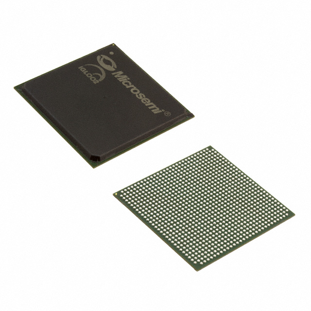
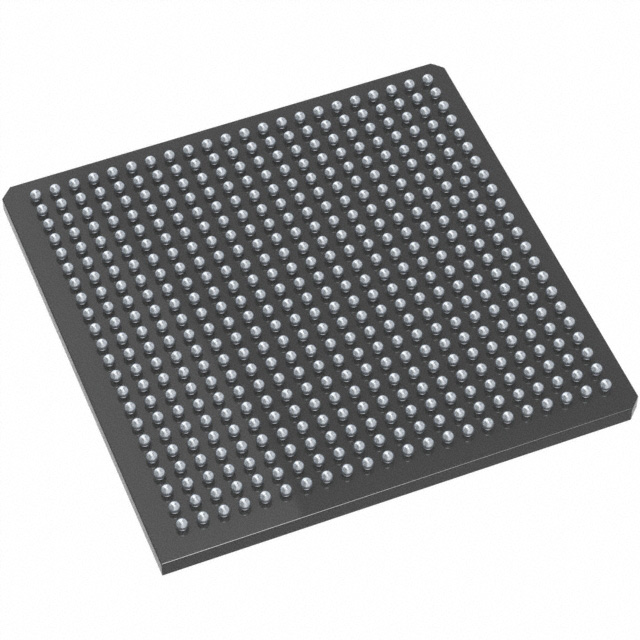
M2GL050-1FGG896
| Part Description |
IGLOO2 Field Programmable Gate Array (FPGA) IC 377 1869824 56340 896-BGA |
|---|---|
| Quantity | 695 Available (as of June 15, 2026) |

| Product Category | Field Programmable Gate Array (FPGA) |
|---|---|
| Manufacturer | Microchip Technology |
| Manufacturing Status | Active |
| Manufacturer Standard Lead Time | 16 Weeks |
| Datasheet |
Specifications & Environmental
| Device Package | 896-FBGA (31x31) | Grade | Commercial | Operating Temperature | 0°C – 85°C | ||
|---|---|---|---|---|---|---|---|
| Package / Case | 896-BGA | Number of I/O | 377 | Voltage | 1.14 V - 2.625 V | ||
| Mounting Method | Surface Mount | RoHS Compliance | ROHS3 Compliant | REACH Compliance | REACH Unaffected | ||
| Moisture Sensitivity Level | 3 (168 Hours) | Number of LABs/CLBs | 56340 | Number of Logic Elements/Cells | 56340 | ||
| Number of Gates | N/A | ECCN | 3A991D | HTS Code | 8542.39.0001 | ||
| Qualification | N/A | Total RAM Bits | 1869824 |
Overview of M2GL050-1FGG896 – IGLOO2 FPGA, 896-BGA
The M2GL050-1FGG896 is a field programmable gate array (FPGA) from the IGLOO2 family integrating fourth-generation flash-based FPGA fabric and high-performance communications interfaces. Designed for applications that require a balance of programmable logic, embedded memory and flexible serial/memory interfaces, this commercial-grade device targets communications, DSP and secure embedded systems.
With 56,340 logic elements and approximately 1.87 Mbits of on-chip RAM, the device emphasizes integration, low-power operation and system-level connectivity while supporting a broad I/O and voltage range for mixed-signal system designs.
Key Features
- Programmable Fabric: Fourth-generation flash-based FPGA fabric with efficient 4-input LUTs and carry chains for increased logic density and performance.
- Logic Capacity: 56,340 logic elements suitable for medium-to-large scale programmable designs.
- Embedded Memory: Total on-chip RAM of 1,869,824 bits (approximately 1.87 Mbits) for local buffering and state storage.
- DSP Resources: Family-level support for fast mathblocks (up to 240) for multiply-accumulate and DSP workloads.
- High-Speed Interfaces: Family support for high-speed serial interfaces including PCI Express, 10 Gbps XAUI/XGMII extensions and native SERDES for multi-gigabit links.
- High-Speed Memory Controllers: Supports DDRx memory controllers (LPDDR/DDR2/DDR3) with features such as command reordering and data reordering for improved memory efficiency (family-level capability).
- User I/Os and Voltage Flexibility: 377 user I/Os with multi-standard I/O support and a supply voltage range of 1.14 V to 2.625 V to accommodate mixed-voltage systems.
- Package and Mounting: 896-ball BGA package (896-FBGA, 31 × 31) designed for surface-mount assembly.
- Operating Conditions and Compliance: Commercial temperature range of 0 °C to 85 °C and RoHS compliant.
- Security and Reliability (Family Features): Design and data security features including encrypted key/bitstream loading, device certificate and anti-tamper capabilities (family-level features).
Typical Applications
- High-Speed Communications: Implement multi-gigabit serial links, PCIe endpoints or 10 Gbps Ethernet PHYs using the device’s native SERDES and protocol support.
- Memory-Intensive Embedded Systems: Use the integrated DDRx memory controllers and on-chip RAM for buffering, frame storage and high-throughput data handling.
- DSP and Signal Processing: Accelerate arithmetic-intensive tasks with the family’s mathblocks and embedded memory for FIR filters, transforms and other DSP functions.
- Secure Embedded Control: Leverage the IGLOO2 family’s design-security features to protect bitstreams and IP in deployed systems.
Unique Advantages
- Highly Integrated FPGA Fabric: Flash-based programmable fabric with 4-input LUTs and carry chains reduces the need for external logic and streamlines board-level design.
- Balanced Logic and Memory: 56,340 logic elements combined with approximately 1.87 Mbits of on-chip RAM supports complex control and data-path functions without excessive external memory.
- Comprehensive Interface Support: Native SERDES, PCIe and DDRx controller support simplifies implementation of high-speed communications and memory interfaces.
- Flexible I/O and Voltage Options: 377 user I/Os and a 1.14 V to 2.625 V supply range enable integration with a wide range of peripherals and voltage domains.
- Commercial-Grade Availability: Surface-mount 896-BGA package and commercial operating range (0 °C to 85 °C) fit a broad set of commercial embedded applications.
- Regulatory Compliance: RoHS compliance supports environmentally conscious manufacturing and supply-chain requirements.
Why Choose M2GL050-1FGG896?
The M2GL050-1FGG896 delivers a combination of substantial programmable logic capacity, embedded memory and family-level high-speed connectivity features in a single, flash-based FPGA device. Its balance of logic elements, on-chip RAM and multi-standard I/O support makes it suitable for communications, DSP and secure embedded applications where integration and predictable operating ranges are important.
Designed for engineers who need a programmable platform with robust memory and interface options, this IGLOO2 device offers scalability across system designs while providing family-level security and high-speed peripheral support to help reduce system BOM and simplify implementation.
Request a quote or submit an inquiry to get pricing and availability for the M2GL050-1FGG896. Our team will assist with technical details and order processing.


Date Founded: 1989
Headquarters: Chandler, Arizona, USA
Employees: 22,000+
Revenue: $8.349 Billion
Certifications and Memberships: ISO9001:2015, IATF16949:2016, AS 9100D


