
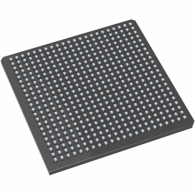
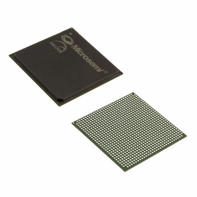
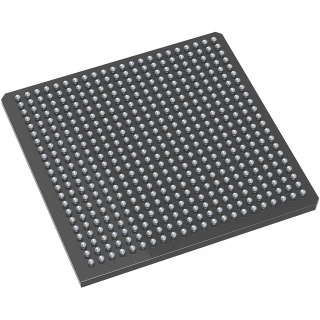
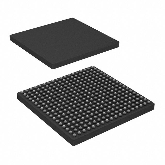
M2GL050T-FG484
| Part Description |
IGLOO2 Field Programmable Gate Array (FPGA) IC 267 1869824 56340 484-BGA |
|---|---|
| Quantity | 1,741 Available (as of October 7, 2026) |
| Product Category | Field Programmable Gate Array (FPGA) |
|---|---|
| Manufacturer | Microchip Technology |
| Manufacturing Status | Active |
| Manufacturer Standard Lead Time | 16 Weeks |
| Datasheet |
Specifications & Environmental
| Device Package | 484-FPBGA (23x23) | Grade | Commercial | Operating Temperature | 0°C – 85°C | ||
|---|---|---|---|---|---|---|---|
| Package / Case | 484-BGA | Number of I/O | 267 | Voltage | 1.14 V - 2.625 V | ||
| Mounting Method | Surface Mount | RoHS Compliance | RoHS non-compliant | REACH Compliance | REACH Unaffected | ||
| Moisture Sensitivity Level | 3 (168 Hours) | Number of LABs/CLBs | 56340 | Number of Logic Elements/Cells | 56340 | ||
| Number of Gates | N/A | ECCN | 3A991D | HTS Code | 8542.39.0001 | ||
| Qualification | N/A | Total RAM Bits | 1869824 |
Overview of M2GL050T-FG484 – IGLOO2 FPGA, 56,340 Logic Elements, 484-BGA
The M2GL050T-FG484 is a flash-based IGLOO2 Field Programmable Gate Array (FPGA) in a 484-BGA package. It combines IGLOO2 fourth-generation FPGA fabric and high-performance communications interfaces to serve designs that require programmable logic, embedded memory and high-speed serial or parallel interfaces.
Designed for commercial applications, this device delivers 56,340 logic elements, approximately 1.87 Mbits of on-chip RAM and 267 user I/Os while operating across a 1.14 V to 2.625 V supply range and a 0 °C to 85 °C temperature range.
Key Features
- Core Logic — 56,340 logic elements (cells) implemented in IGLOO2 flash-based FPGA fabric with efficient 4-input LUTs and carry chains for balanced performance and power.
- Embedded Memory — Approximately 1.87 Mbits of total on-chip RAM; IGLOO2 architecture supports multiple embedded memory options including large dual-port SRAM and micro SRAM blocks.
- DSP & Math Resources — IGLOO2 family provides dedicated mathblocks for DSP functions; the architecture includes high-performance signed and unsigned multipliers and accumulators as part of the family feature set.
- High-Speed Serial Interfaces — IGLOO2 architecture supports multi-lane SERDES and protocol-capable interfaces including PCIe and XAUI/XGMII extensions for high-speed communication needs.
- High-Speed Memory Interfaces — Family-level support for DDR/DDR2/DDR3 memory controllers, enabling interfaces to external high-speed memories when required by system design.
- I/O Flexibility — 267 user I/Os with multi-standard support across a wide range of signaling standards (LVCMOS, DDR I/Os, LVDS family, etc.) as described for the IGLOO2 family.
- Package & Mounting — 484-ball BGA (supplier device package: 484-FPBGA, 23×23) optimized for surface-mount assembly.
- Power & Temperature — Core and I/O supply range from 1.14 V to 2.625 V and commercial operating temperature from 0 °C to 85 °C.
- Security & Reliability Features — IGLOO2 family-level security includes encrypted bitstream loading and supply-chain device certificate options; family also emphasizes low-power and reliability characteristics.
- Compliance — RoHS-compliant for environmental and regulatory conformity.
Typical Applications
- High-speed communications — Implements protocol bridging, SERDES interfacing and PCIe endpoints using the IGLOO2 family’s serial and protocol-capable interfaces.
- Embedded compute and DSP — Uses mathblocks and on-chip RAM for signal processing, filtering and arithmetic-intensive tasks in compact FPGA-based subsystems.
- Memory interface controllers — Acts as a controller or interface logic for DDR/LPDDR/DDR2/DDR3 memories leveraging family DDR controller support.
- Secure embedded systems — Suitable for applications requiring encrypted bitstream loading and hardware-based anti-tamper or device authentication features provided by the IGLOO2 architecture.
Unique Advantages
- High integration density: 56,340 logic elements and substantial on-chip RAM reduce external component count and simplify board-level design.
- Multi-protocol connectivity: Family support for SERDES lanes and PCIe/XAUI interfaces enables flexible high-speed link implementation.
- Embedded memory options: Multiple SRAM block types and on-chip eSRAM/eNVM options in the IGLOO2 architecture streamline data buffering and code storage.
- Security-focused architecture: Encrypted bitstream loading and device authentication capabilities help protect IP and enable secure deployment models.
- Commercial temperature and broad supply range: 0 °C to 85 °C operating range and 1.14 V–2.625 V supply tolerance support a wide set of commercial designs and board topologies.
- RoHS compliance: Environmentally compliant manufacturing and materials for regulated markets.
Why Choose M2GL050T-FG484?
The M2GL050T-FG484 brings IGLOO2 family capabilities—flash-based FPGA fabric, extensive embedded memory, DSP resources and high-speed serial interfaces—into a single commercial-grade 484-BGA device. Its combination of 56,340 logic elements, approximately 1.87 Mbits of RAM and 267 I/Os targets designs that need programmable logic density alongside secure, low-power operation.
This device suits engineering teams building communication subsystems, DSP-accelerated embedded controllers, or secure programmable platforms that benefit from integrated memory and configurable high-speed I/O while maintaining commercial temperature and supply requirements.
Request a quote or submit an inquiry to learn more about pricing, availability and how the M2GL050T-FG484 can fit your next design.





















Date Founded: 1989
Headquarters: Chandler, Arizona, USA
Employees: 22,000+
Revenue: $8.349 Billion
Certifications and Memberships: ISO9001:2015, IATF16949:2016, AS 9100D




